Light emitting device package

a technology of light-emitting devices and light-emitting devices, which is applied in the direction of semiconductor/solid-state device manufacturing, semiconductor devices, electrical devices, etc., can solve the problems of increased manufacturing cost, difficulty in increasing light extraction efficiency, and waste of effort and assembly costs, so as to improve light extraction efficiency and heat dissipation performance, the effect of simplifying the structur

Active Publication Date: 2006-12-21
SAMSUNG ELECTRONICS CO LTD
View PDF7 Cites 79 Cited by
  • Summary
  • Abstract
  • Description
  • Claims
  • Application Information

AI Technical Summary

Benefits of technology

[0007] The present invention may provide a light emitting device package having a simplified str

Problems solved by technology

The package parts such as the heat sink 15, the package body 10 and the plastic lens 50 are formed of different materials, so that there are complexities in the prior art in that a number of processes are required to manufacture the package, and the manufacturing cost is increased.
Another complication of t

Method used


Image

  • Light emitting device package
  • Light emitting device package
  • Light emitting device package

Examples


first embodiment

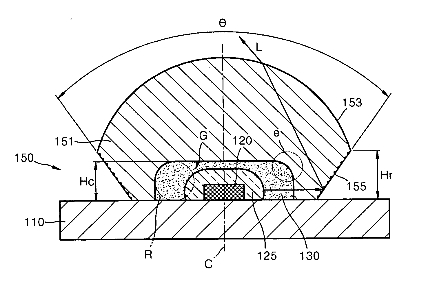
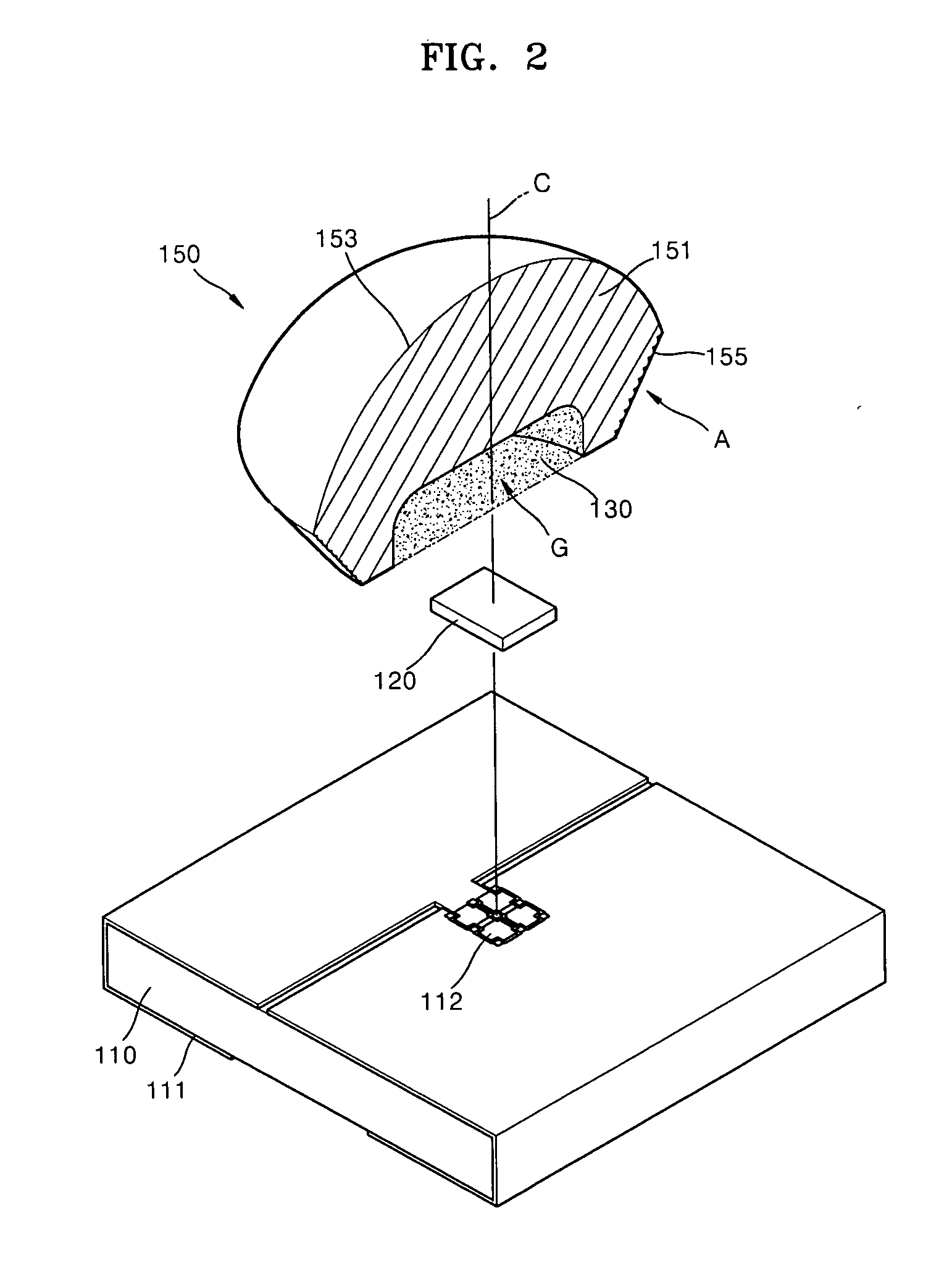
[0031] A light emitting device package of the present invention will now be described more fully with reference to the accompanying drawings, in which preferred exemplary embodiments of the invention are shown. FIG. 2 is an exploded perspective view of the light emitting device package according to the present invention. Referring to this drawing, the light emitting device package includes a base substrate 110 on which a wiring pattern 111 is formed, a light emitting device 120 mounted on the base substrate 110 to emit light when supplied with power via the wiring pattern 111, a molded lens 150 stably seated on the base substrate 110 to cover the light emitting device 120 and extract light emitted from the light emitting device 120 with high efficiency, and a sealing resin 130 injected into an inner space G between the molded lens 150 and the base substrate 110 to bond the molded lens 150 to the base substrate 110. The light emitting device 120 includes an electrode pattern (not sho...

second embodiment

[0042]FIG. 5 is a perspective view of a light emitting device package according to the present invention. Referring to this, a light emitting device 220 is packaged between a base substrate 210 and a molded lens 250. A sealing resin 230 is injected into an inner space G which contains the light emitting device 220, to bond the base substrate 210 to the molded lens 250. A transparent body 251 of the molded lens 250 has a transmission surface 253 through which light is emitted from the light emitting device 220, and a reflective surface 255 inclined inward from the transmission surface 253.

[0043] In this embodiment, unlike the first embodiment, a separate sub-mount 240 is interposed between the light emitting device 220 and the base substrate 210. The sub-mount 240 physically and electrically bonds the light emitting device 220 to the base substrate 210. To this end, the sub-mount 240 may first be flip-chip bonded to the base substrate 210 below and then flip-chip bonded to the light ...


PUM


Abstract

A light emitting device package is provided. The light emitting device package comprises a base substrate on which a wiring pattern is formed; a light emitting device mounted on the base substrate to emit light when supplied with driving power through the wiring pattern; a molded lens stably seated on the base substrate and having an inner space for sealing the light emitting device and reflective surfaces formed along outer sides facing the inner space to guide light from the light emitting device in an effective display direction; and a sealing resin between the inner space to bond the base substrate to the molded lens, whereby the packaging structure is simplified so that an assembly process and reliability testing are simplified, process losses due to defects are minimized, and the light extraction efficiency from the light emitting device and heat-dissipation performance are improved.

Description

CROSS-REFERENCE TO RELATED PATENT APPLICATION [0001] This application claims the benefit of Korean Patent Application No. 10-2005-0052578, filed on Jun. 17, 2005, in the Korean Intellectual Property Office, the disclosure of which is incorporated herein in its entirety by reference. BACKGROUND OF THE DISCLOSURE [0002] 1. Field of the Disclosure [0003] The present disclosure relates to a light emitting device package, and more particularly, to a light emitting device package having a simple improved structure which provides a higher light extraction efficiency and heat-dissipation performance, and minimizes process losses due to defects. [0004] 2. Description of the Related Art [0005]FIG. 1 illustrates the sectional structure of a light emitting diode (LED) package of the prior art. Referring to FIG.1, the LED package includes an LED as a light emitting device 20, a heat sink 15 on which the light emitting device 20 is mounted, and a sub-mount 40 between the light emitting device 20 ...

Claims


Application Information

Patent Timeline
IPC IPC(8): H01L33/00H01L33/58H01L33/60
CPCH01L33/58H01L33/60H01L2924/0002H01L2924/00
Inventor KIM, HYUNG-KUNKIM, YU-SIK
Owner SAMSUNG ELECTRONICS CO LTD
Why Eureka
Try Eureka