Process for holding strain in an island etched in a strained thin layer and structure obtained by implementation of this process

a thin layer and island technology, applied in the field of structures, can solve the problems of no longer being homogeneous within the island, the thickness of the strained layer is limited to a critical thickness, and the stress in the island will no longer be the same,

Inactive Publication Date: 2006-12-21
S O I TEC SILICON ON INSULATOR THECHNOLOGIES
View PDF19 Cites 10 Cited by
  • Summary
  • Abstract
  • Description
  • Claims
  • Application Information

AI Technical Summary

Benefits of technology

[0013] More particularly, this invention can advantageously be used for applications in the process for manufacturing integrated circuits (and particularly for manufacturing CMOS components) during which a thick oxide layer is formed conventionally (by oxidation of the substrate, typically made of silicon) or a layer made of dielectric material is...

Problems solved by technology

It is known that the thickness of the strained layer is limited to a critical thickness beyond which plastic relaxation of the strain is observed because of the formation of dislocation type defects.
In other words, there is a risk that the stress in the is...

Method used


Image

  • Process for holding strain in an island etched in a strained thin layer and structure obtained by implementation of this process
  • Process for holding strain in an island etched in a strained thin layer and structure obtained by implementation of this process
  • Process for holding strain in an island etched in a strained thin layer and structure obtained by implementation of this process

Examples


Embodiment Construction

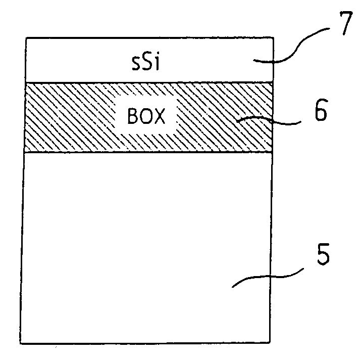
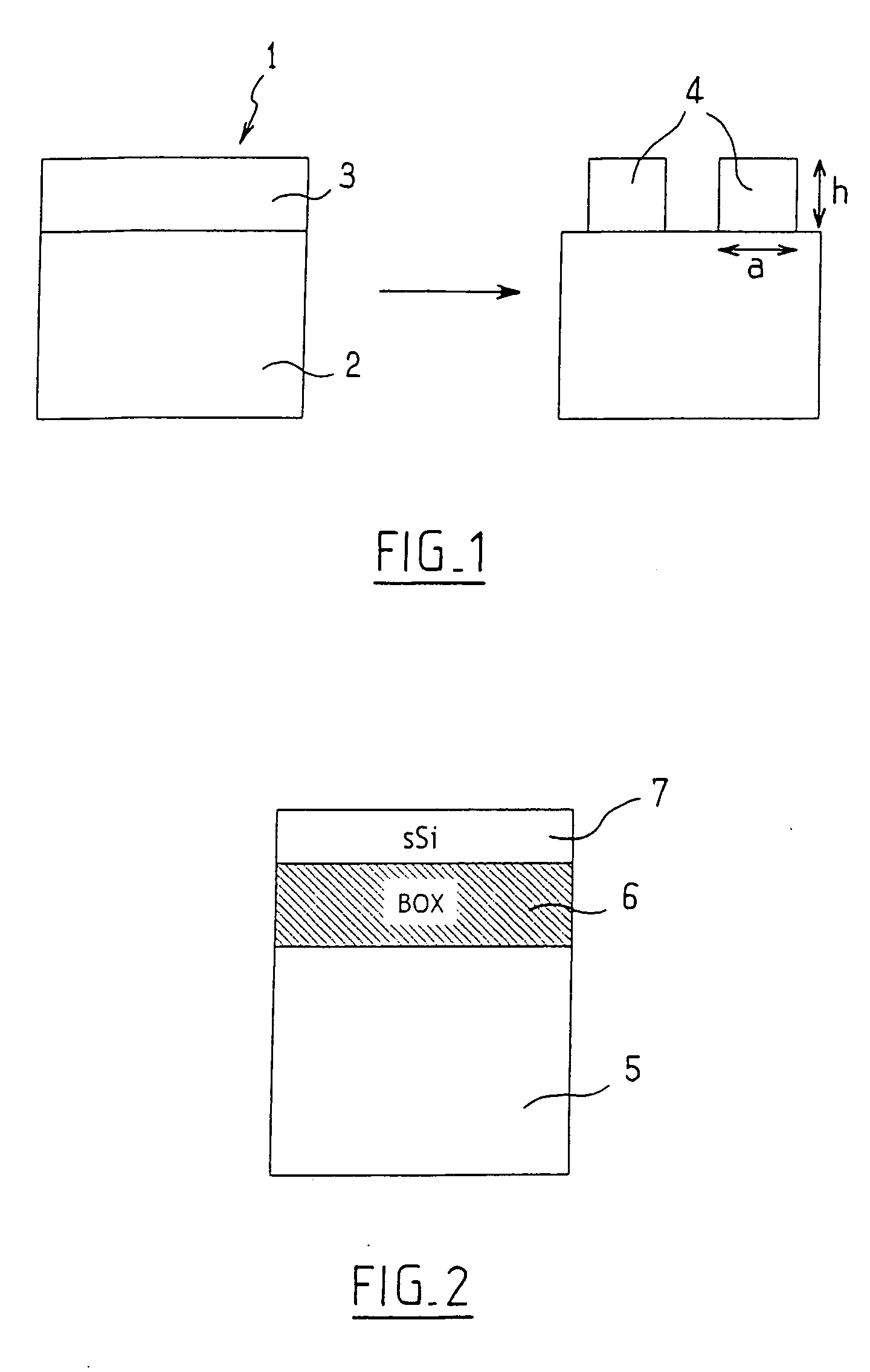
[0034] With reference to FIG. 1, the figure shows a structure 1 comprising a substrate 2 and a thin layer 3 made of a strained semiconducting material on the substrate 2. During a step of manufacturing electronic components, a set of islands 4 is formed from the thin strained semiconducting layer 3. The islands 4 will form conducting regions for electronic components. The islands 4 are typically formed by etching the thin layer 3 in a particular pattern. It should be noted that this etching may be chemical etching or Reactive Ion Etching (RIE).

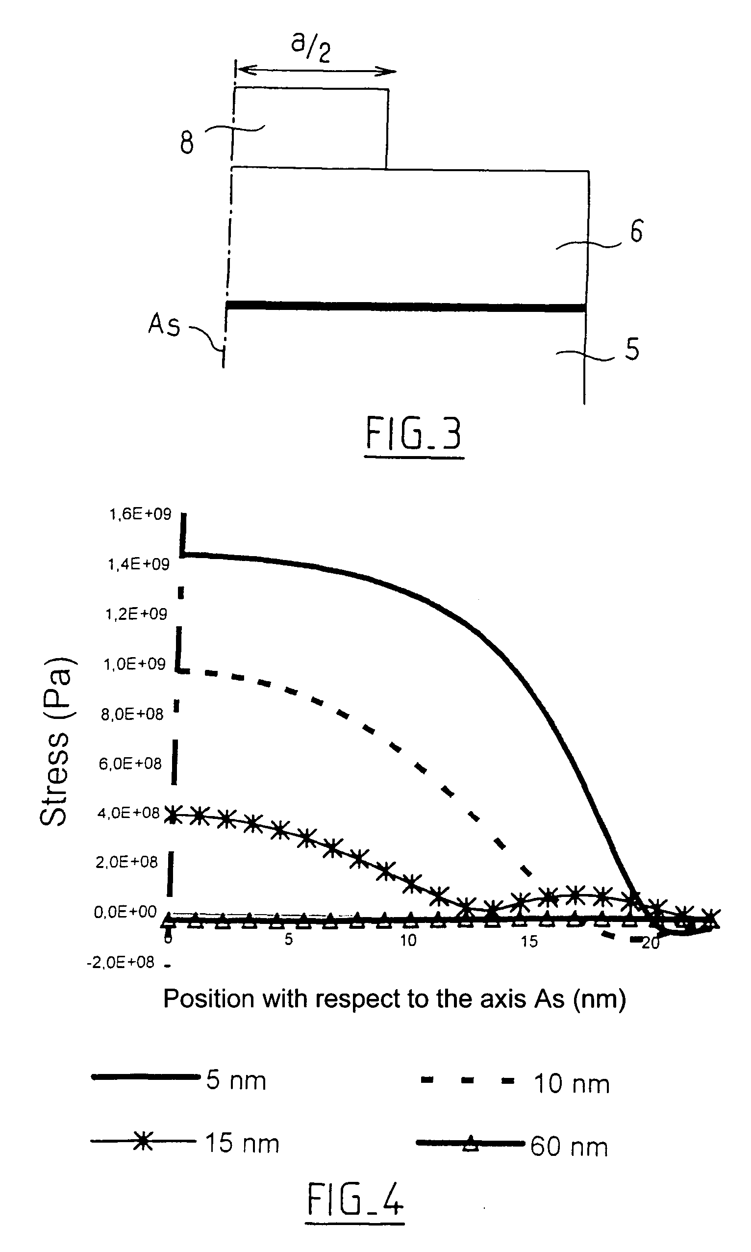
[0035] The following description is initially intended to analyse the stress relaxation in the islands following etching the thin layer during the manufacturing of electronic components.

[0036] Etching of the strain layer was simulated by making a finite element model so as to quantify stress relaxation phenomena within the layer “cut-out” by etching the thin layer to form an island. More precisely, this simulation studies the relaxation with...


PUM


Abstract

The invention relates to structures useful for the manufacture of electronic components, which comprise a substrate, a strain holding layer, and a layer of a strained semiconducting material. These structures are particularly useful where islands are later formed in the strained semiconducting material because the strain holding layer limits relaxation of stress in the islands. This invention also relates to processes for making a these structures.

Description

FIELD OF THE INVENTION [0001] The field of the invention related to structures comprising a substrate with a thin layer of a strained semiconducting material, the thin layer acting as an active layer for the formation of electronic components. BACKGROUND [0002] Semiconductor structures a strained active layer on the surface of a substrate have advantageous electrical properties. Since the crystalline network of the electrically active layer is strained, the mobility of electric charges (electrons, holes) is effectively increased over the entire active layer as compared to an unstrained layer. The result is an increase of the order of 20 to 30% in the performance of the transistors that will be formed from the strained layer. [0003] It is known that the thickness of the strained layer is limited to a critical thickness beyond which plastic relaxation of the strain is observed because of the formation of dislocation type defects. Care must be taken in this invention not to form a thin...

Claims


Application Information

Patent Timeline
IPC IPC(8): H01L27/12
CPCH01L21/02381H01L21/02488H01L29/7843H01L21/84H01L29/7842H01L21/02532
Inventor BOUSSAGOL, ALICECAYREFOURCQ, IAN
Owner S O I TEC SILICON ON INSULATOR THECHNOLOGIES
Why Eureka
Try Eureka