
Flash memory and fabrication method thereof

a technology of flash memory and fabrication method, which is applied in the field of flash memory, can solve the problems of reducing the dimension of semiconductor memory and the area of flash memory cannot be further shaved, and achieve the effect of reducing the contact area connected to the drain area

Inactive Publication Date: 2006-12-21
MACRONIX INT CO LTD
View PDF4 Cites 7 Cited by
  • Summary
  • Abstract
  • Description
  • Claims
  • Application Information

AI Technical Summary

Benefits of technology

[0016] According to the method of fabricating the flash memory of an embodiment of the present invention, the step of filling the isolation layer between the first conductive layers comprises: a dielectric layer is formed over the substrate by a high-density plasma process, and the dielectric layer is removed by a chemical-mechanical polish (CMP) process until the top of the first conductive layers is exposed. Then, it is optional to remove a portion of the high-density plasma material layer so that the top of the high-density plasma material layer is higher than the top of the first conductive layers to enhance the gate coupling ratio (GCR).
[0020] According to the present invention, the flash memory has the control gates and the doped regions, which are alternately disposed. As a result, the contact areas connected to the drain areas are reduced, and the whole array areas shrink as well. Additionally, signals can be transmitted with the same distance. In addition, the fabrication method of the present invention is compatible with the traditional process. Without additional processes, the flash memory of the present invention can be fabricated.

Problems solved by technology

As a result, the area of the flash memory cannot further shrink.
It is an obstacle in reducing the dimension of the semiconductor memory.

Method used


Image

  • Flash memory and fabrication method thereof
  • Flash memory and fabrication method thereof
  • Flash memory and fabrication method thereof

Examples


first embodiment

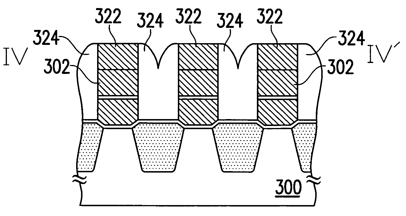
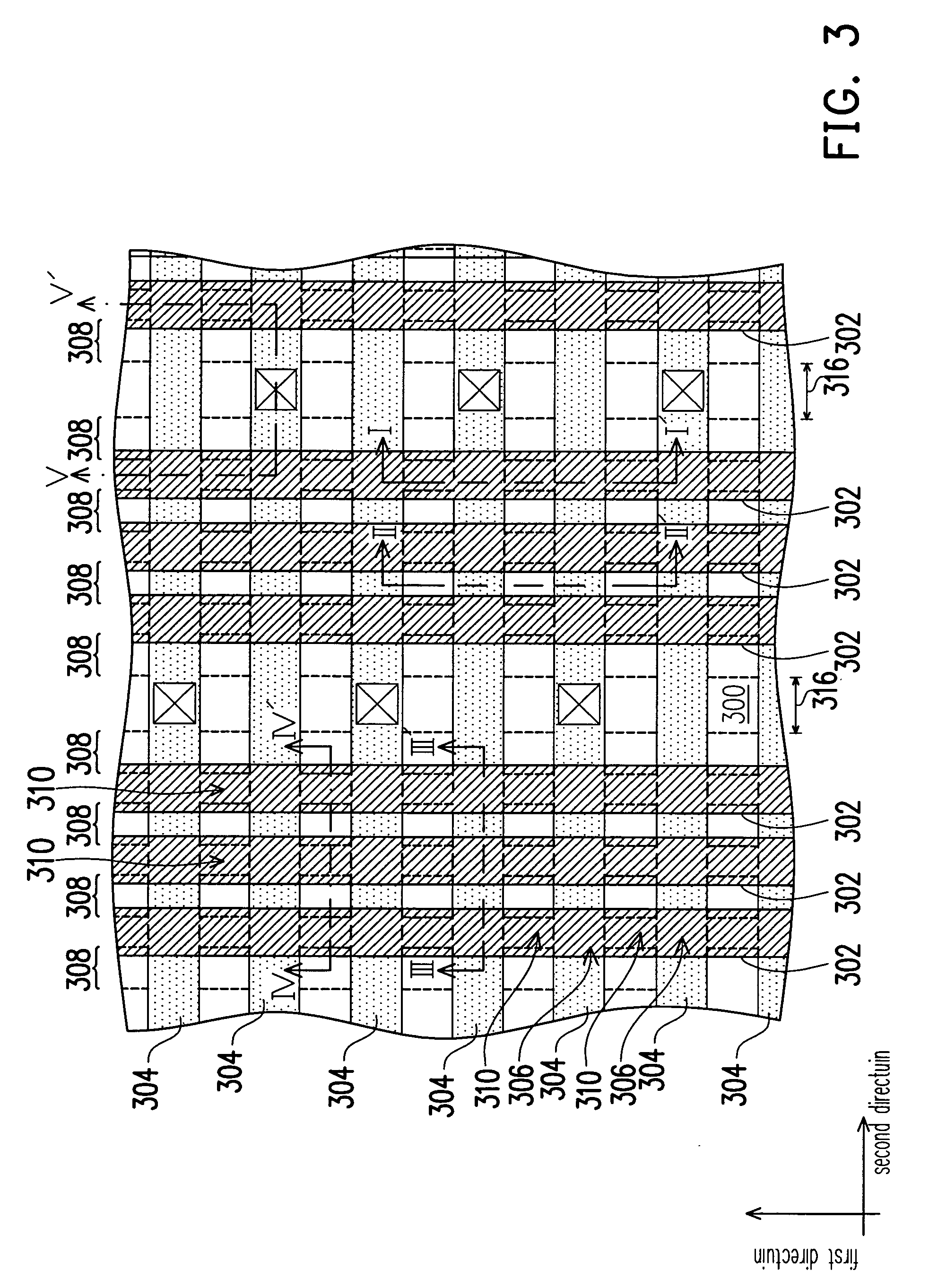
[0031]FIG. 3 is a top view of a flash memory according to the first embodiment of the present invention. FIGS. 4-I, 4-II, 4-III, and 4-IV are cross sectional views of the flash memory along I-I′, II-II′, III-III′, and IV-IV′, respectively.

[0032] Referring to FIGS. 3, 4-I, 4-II, 4-III, and 4-IV, the flash memory comprises the substrate 300, plural strips of control gates 302, a plurality of doped regions 304, the isolation layer 306, a plurality of isolation structures 308, a plurality of floating gates 310, a plurality of tunneling dielectric layers 312 and a plurality of inter-gate dielectric layers 314. Wherein, the control gates 302 are arranged with a first direction over the substrate 300. The doped regions 304 are arranged within the substrate with a second direction within the substrate 300. In the flash memory of this embodiment, the doped regions 304 serve as sources and drains. Moreover, the isolation layer 306 is disposed between the control gates 302 and the doped regio...

second embodiment

[0037] Following are descriptions of the method of fabricating the flash memory. These descriptions are mere an embodiment of the present invention. The present invention, however, is not limited thereto. Moreover, main device references used in this embodiment represent that they are similar to those in the last embodiment.

[0038] FIGS. 6A-I-6D-I are cross sectional views of process of fabricating the structure of FIG. 3 along I-I′. FIGS. 6A-II-6E-II are cross sectional views of process of fabricating the structure of FIG. 3 along II-II′. FIGS. 6A-III-6E-III are cross sectional views of process of fabricating the structure of FIG. 3 along III-III′. FIGS. 6A-IV-6E-IV are cross sectional views of process of fabricating the structure of FIG. 3 along IV-IV′.

[0039] Referring to FIG. 6A-I-6A-IV, plural strips of trench isolation structures 608 with the first direction are formed within the substrate 300 as shown in FIG. 3. The tunneling dielectric layer 312 then is formed over the subst...


PUM


Abstract

A flash memory comprises a substrate, control gates, doped regions, an isolation layer, isolation structures, floating gates, tunneling dielectric layers and inter-gate dielectric layers. The control gates are arranged over the substrate with a first direction, and the doped regions are arranged within the substrate with a second direction. The isolation layers are disposed between the control gates and the doping regions, and the isolation structures are disposed within the substrate where the doped regions and the control gates do not overlap. Furthermore, the floating gates are disposed between the control gates and the substrate that is not covered by the isolation layers. The tunneling dielectric layers are disposed between the substrate and the floating gates. The inter-gate dielectric layers are disposed between the control gates and the floating gates.

Description

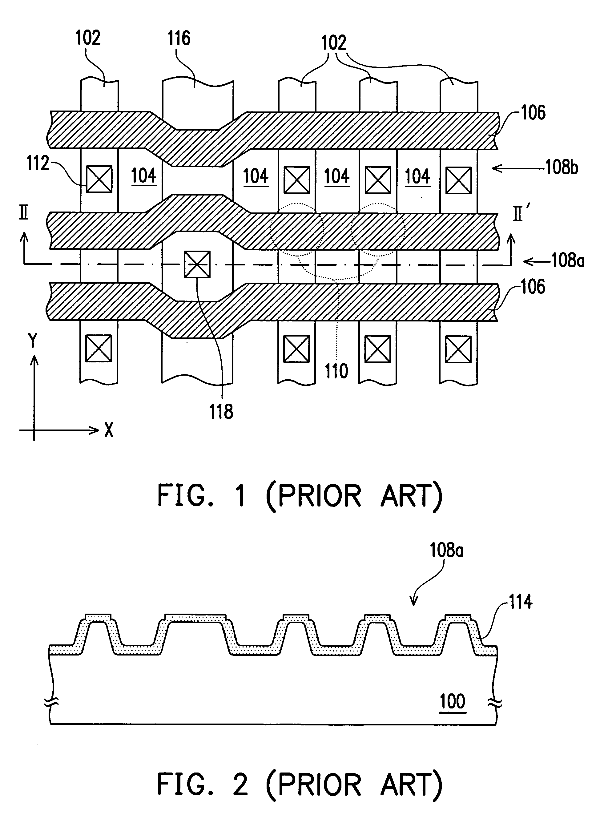
BACKGROUND OF THE INVENTION [0001] 1. Field of the Invention [0002] The present invention relates to a flash memory, and more particularly, to a flash memory and its fabrication method. [0003] 2. Description of the Related Art [0004] Since a flash memory can store, read or erase data at multiple times, even if power is cut off, the data stored in the memory will not be erased. Accordingly, it becomes a widely adopted non-volatile memory device in the fields of personal computers and electronic apparatuses. [0005]FIG. 1 is a top view of a prior art flash memory. FIG. 2 is a cross sectional view of the structure along II-II′ in FIG. 1. [0006] Referring to FIGS. 1 and 2, the active regions 102 and the isolation structures 104 are alternately disposed within the substrate 100 with the y direction. The control gates 106 are arranged over the substrate 100 with the x direction. The floating gates (not shown) of the memory cell and the tunneling dielectric layers (not shown) are disposed a...

Claims


Application Information

Patent Timeline
IPC IPC(8): H01L29/76H01L21/8236
CPCH01L27/11521H01L27/115H10B69/00H10B41/30
Inventor LIN, HSIN-FUWU, CHUN-PEI
Owner MACRONIX INT CO LTD
Learn More