Supercharge Your Innovation With Domain-Expert AI Agents!

Thin film transistor array panel and liquid crystal display including the same

a technology of thin film transistors and array panels, which is applied in the direction of instruments, semiconductor devices, optics, etc., can solve the problems of slowed response speed of display devices and complicated manufacturing of lcds

Inactive Publication Date: 2006-12-21
SAMSUNG DISPLAY CO LTD
View PDF6 Cites 2 Cited by
  • Summary
  • Abstract
  • Description
  • Claims
  • Application Information

AI Technical Summary

Benefits of technology

The present invention provides an LCD with a wide viewing angle without forming cutouts or protrusions in the common electrode. A thin film transistor drives a pixel electrode having a cutout and a direction control electrode connected to the thin film transistor overlaps the pixel electrode's cutout. A coupling electrode is connected to the direction control electrode. The voltage applied to the direction control electrode is higher than the voltage of the pixel electrode. This results in a stronger horizontal component of a subordinate electric field and in the opposite direction to the horizontal component of the primary electric field, which makes the pure horizontal component of the electric field at the cutout where the direction control electrode is located in the same direction as the horizontal component at the edge of the adjacent pixel electrode.

Problems solved by technology

The manufacturing of the LCD is complicated because of the additional process step for forming the protrusions.
Moreover, the VA mode LCD having protrusions or cutouts has a problem in that the response speed of the display device is slowed since the LC molecules far from the protrusions or cutouts are under weak control while the LC molecules near the protrusions or cutouts are strongly controlled.

Method used


Image

  • Thin film transistor array panel and liquid crystal display including the same
  • Thin film transistor array panel and liquid crystal display including the same
  • Thin film transistor array panel and liquid crystal display including the same

Examples


Embodiment Construction

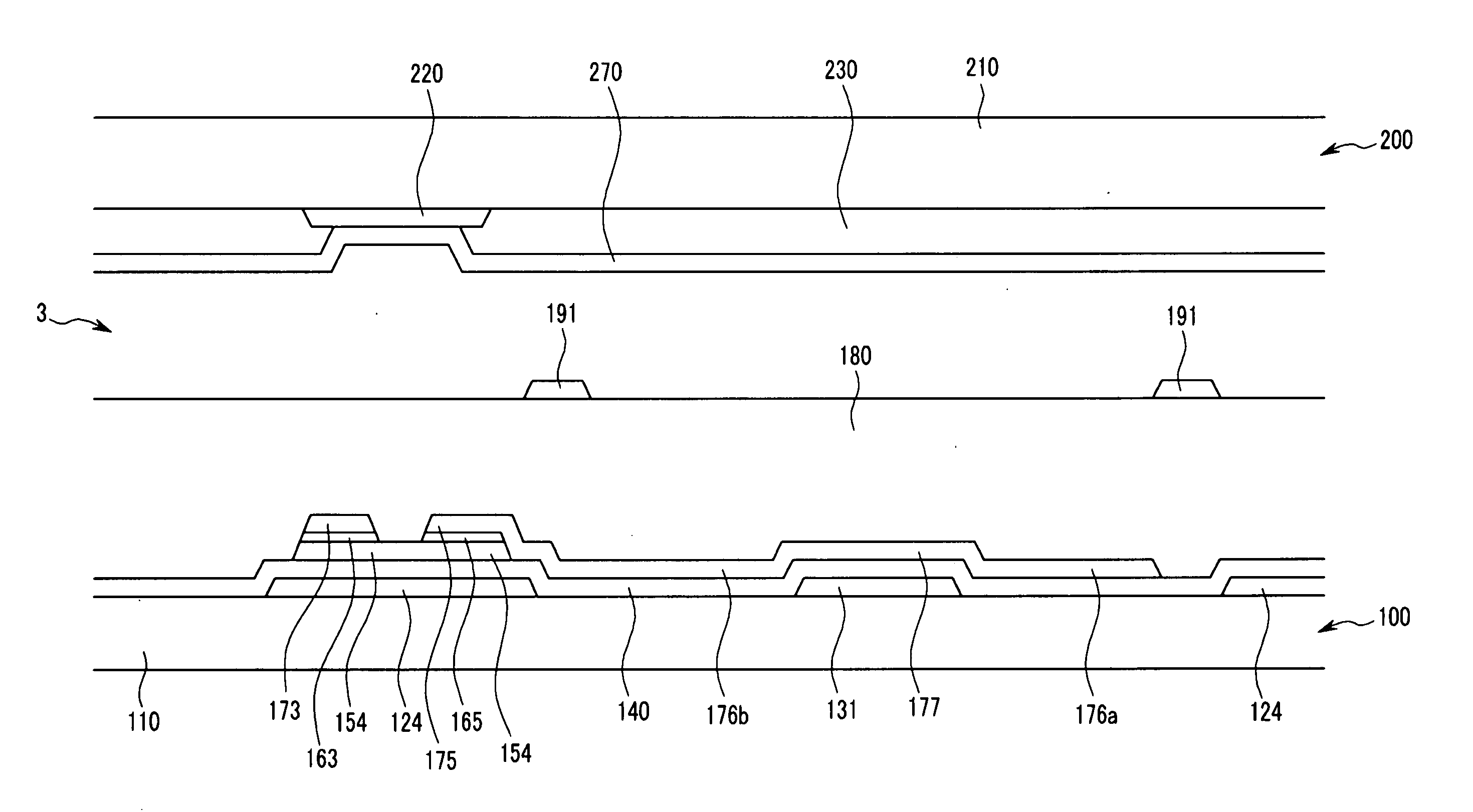
[0011] In the drawings, the thickness of layers, films, and regions are exaggerated for clarity. Like numerals refer to like elements throughout. It will be understood that when an element such as a layer, film, region, or substrate is referred to as being “on” another element, it can be directly on the other element or intervening elements may also be present. In contrast, when an element is referred to as being “directly on” another element, there are no intervening elements present.

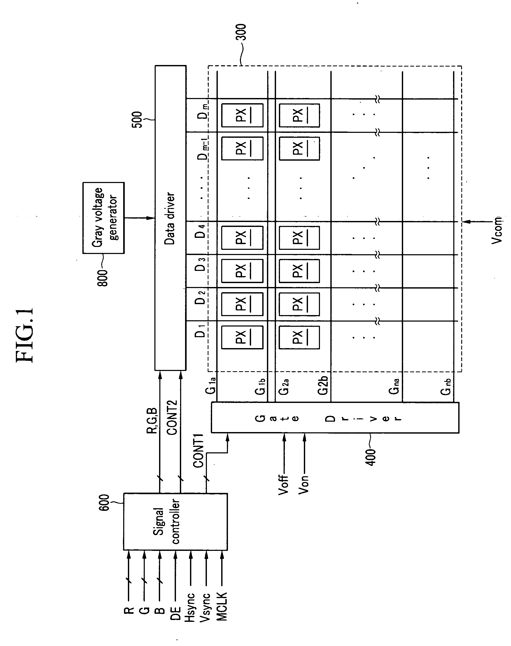
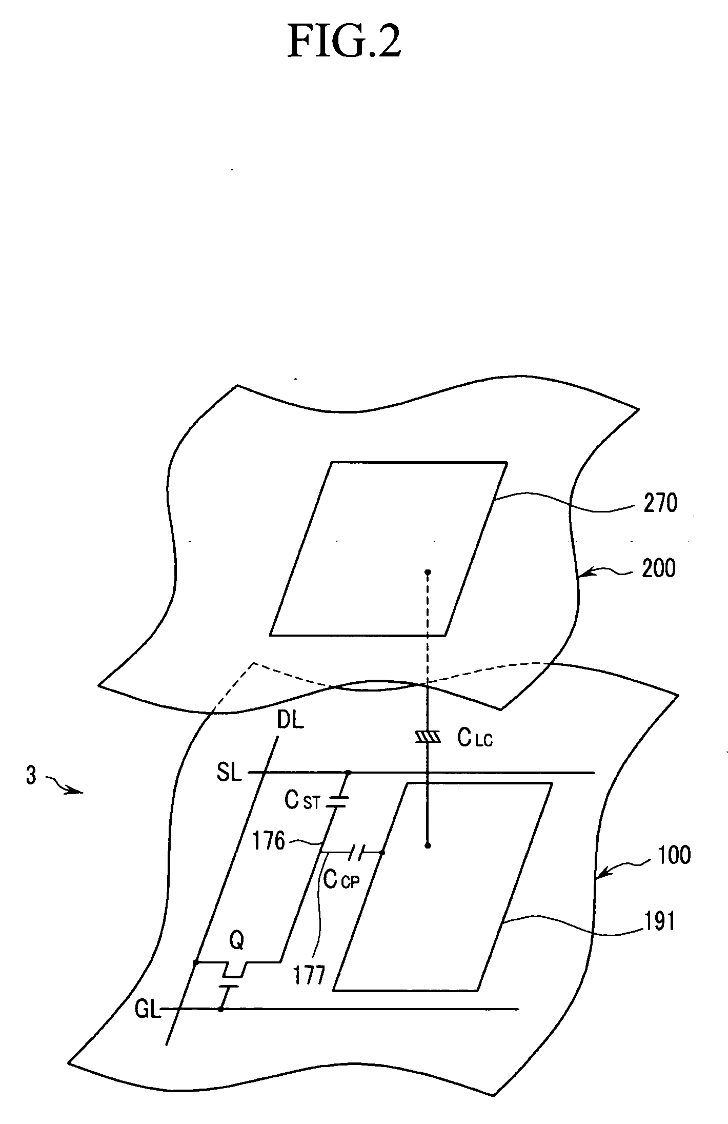
[0012]FIG. 1 is a block diagram of an LCD according to an embodiment of the present invention, and FIG. 2 is an equivalent circuit diagram of a pixel of an LCD according to an embodiment of the present invention. Referring to FIGS. 1 and 2, the LCD according to an embodiment of the present invention includes a liquid crystal panel assembly 300, a gate driver 400 and a data driver 500 that are connected to the liquid crystal panel assembly 300, a gray voltage generator 800 connected to the data driver ...


PUM

PropertyMeasurementUnit
inclination angleaaaaaaaaaa
inclination anglesaaaaaaaaaa
dielectric constantaaaaaaaaaa

Abstract

The present invention provides a VA mode LCD having a wide viewing angle without forming cutouts or protrusions in the common electrode. A thin film transistor drives a pixel electrode having a cutout and a direction control electrode connected to the thin film transistor overlaps the pixel electrode's cutout. A coupling electrode is connected to the direction control electrode overlapping the pixel electrode allowing the direction control electrode voltage to be maintained higher than the pixel electrode voltage.

Description

REFERENCE TO RELATED APPLICATION [0001] This application claims priority and benefit of Korean Patent Application No. 10-2005-0052954 filed in the Korean Intellectual Property Office on Jun. 20, 2005, the contents of which are incorporated herein by reference. FIELD OF THE INVENTION [0002] The present invention relates to a thin film transistor (TFT) array panel for a liquid crystal display. DESCRIPTION OF THE RELATED ART [0003] A liquid crystal display (LCD) generally includes an upper panel provided with a common electrode and color filters, a lower panel provided with thin film transistors (TFTs) and pixel electrodes, and a liquid crystal (LC) layer interposed therebetween. The pixel electrodes and the common electrode are supplied with different voltages to generate an electric field in the LC layer that determine the orientations of the LC molecules. Hereinafter, the pixel electrode 191 and the common electrode 270 may be referred to as electric field generating electrodes. Sin...

Claims


Application Information

Patent Timeline
Patent Type & Authority Applications(United States)
IPC IPC(8): G02F1/136
CPCG02F1/136213H01L27/1255G02F1/1393G02F1/1343
Inventor SHIN, KYOUNG-JU
Owner SAMSUNG DISPLAY CO LTD
Features
  • R&D
  • Intellectual Property
  • Life Sciences
  • Materials
  • Tech Scout
  • Unparalleled Data Quality
  • Higher Quality Content
  • 60% Fewer Hallucinations
Learn More