Optical modulation element array

a technology arrays, applied in the field of optical modulation element arrays, can solve the problems of small area of micro-mirrors, and large ineffective area generated to lower aperture ratio, so as to maintain the aperture ratio of optical modulation elements, the effect of reducing the twist elastic coefficien

Inactive Publication Date: 2006-12-21
FUJIFILM CORP +1
View PDF7 Cites 81 Cited by
  • Summary
  • Abstract
  • Description
  • Claims
  • Application Information

AI Technical Summary

Benefits of technology

[0019] The invention has been made in consideration of these circumstances. It is an object of the invention to provide an optical modulation element array capable of lengthening a hinge without enlarging a micro mirror so that the aperture ratio in an optical modulation element can be secured, and an operation performed at a low voltage can be accomplished while preventing a decrease in displacement responsibility.
[0023] According to the optical modulation element array described in the item (1) or (2), the optical modulation elements are arranged so that optical modulation elements next to each other are shifted in the first direction (hereinafter also simply referred to as a zigzag alignment), and the end of the hinge provided in parallel with the second direction is disposed in a gap between the optical modulation elements adjoining along the first direction. Therefore, each of the hinges adjoining in the second direction never interferes with each other. In other words, since the hinge is disposed in a gap between the optical modulation elements adjoining along the second direction, each of the ends of the hinge never come into contact with each other. As a result, the hinge can be lengthened without enlarging the optical function film.
[0025] According to the optical modulation element array described in the item (3), the optical function film can be floated and disposed above the hinge and the first support. In other words, a space in which only the optical function film can be disposed is secured on the upper layer differing from the lower layer on which the hinge and the first support are disposed. Therefore, a space to dispose the hinge and the first support and the area of the optical function film can be made larger, and optical efficiency in optical modulation can be made higher than in the conventional structure in which the hinge, the first support, and the optical function film are disposed on the same plane.
[0027] According to the optical modulation element array described in the item (4), the optical function film is connected to the hinge through the second support, and the elastic coefficient exhibited when the optical function film operates while rotating is restricted to a small value. Therefore, the optical modulation element array can be driven at a low voltage, and can respond at a high speed. Additionally, since the length of the hinge in the axial direction can be further increased, the low-voltage drivability and the rapid responsibility can be improved.
[0029] According to the optical modulation element array described in the item (5), an electrostatic force is generated between the electrode layers and the fixed electrodes. This electrostatic force is used as the displacement drive source of the optical function film. In other words, the movable film that is nearer to the substrate than to the optical function film is allowed to generate an electrostatic force, and hence a greater electrostatic force can be obtained. Therefore, drivability at a lower voltage can be achieved, and the optical function film can respond at a greater speed.
[0032] According to an as aspect of the invention, the optical modulation elements is arranged in a zigzag alignment, and the end of the hinge provided in parallel with the second direction is disposed in a gap between the optical modulation-element adjoining along the first direction. Therefore, the hinge can be lengthened without enlarging the optical function film. In other words, the hinge can be lengthened while maintaining the aperture ratio of the optical modulation elements, and the twist elastic coefficient thereof can be reduced. As a result, low-voltage drivability can be achieved while preventing a decrease in displacement responsibility.

Problems solved by technology

As a result, disadvantageously, a large ineffective area 13 will be generated to lower the aperture ratio.
However, there are limitations on a decrease in Young's modulus of hinge film material, a decrease in hinge thickness, and a decrease in hinge width.
However, since the micro mirror and the hinge are disposed on the same plane, the area of the micro mirror becomes small after all if the hinge is lengthened.

Method used


Image

  • Optical modulation element array
  • Optical modulation element array
  • Optical modulation element array

Examples


first embodiment

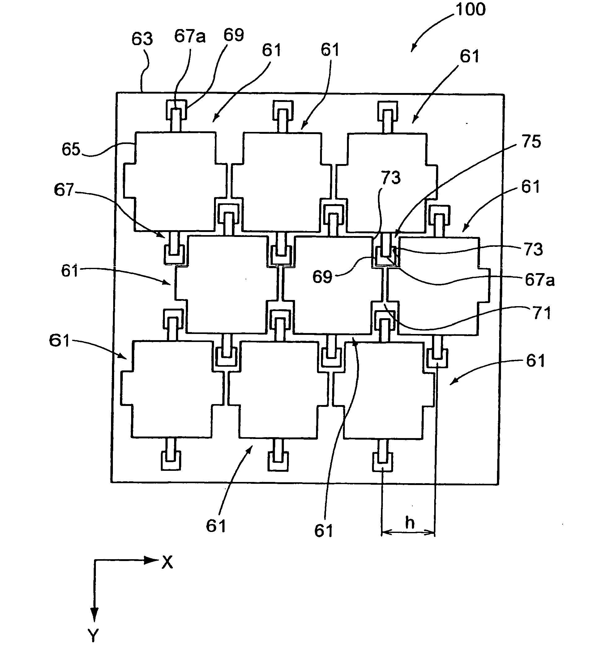
[0047]FIG. 1 is a plan view of an optical modulation element array in which optical modulation elements using micro mirrors serving as optical function films are arranged in a zigzag alignment.

[0048] The optical modulation element array 100 according to this embodiment includes an array of optical modulation element 61. The optical modulation element 61 includes a micro mirror 65 serving as an optical function film provided above a substrate 63, a hinge 67 supporting the micro mirror 65 so that the micro mirror 65 can be tilted, and a first support 69 by which an end 67a of the hinge 67 is connected to the substrate 63.

[0049] In the optical modulation element 61, an electrode layer, not shown, is provided on the micro mirror 65, and a pair of fixed electrodes, not shown, disposed on either side of the hinge 67 are provided on the substrate 63. In the optical modulation element 61, the micro mirror 65 is driven by the pair of fixed electrodes. The micro mirror 65 undergoes an elect...

second embodiment

[0055] Next, the optical modulation element array according to the invention will be described.

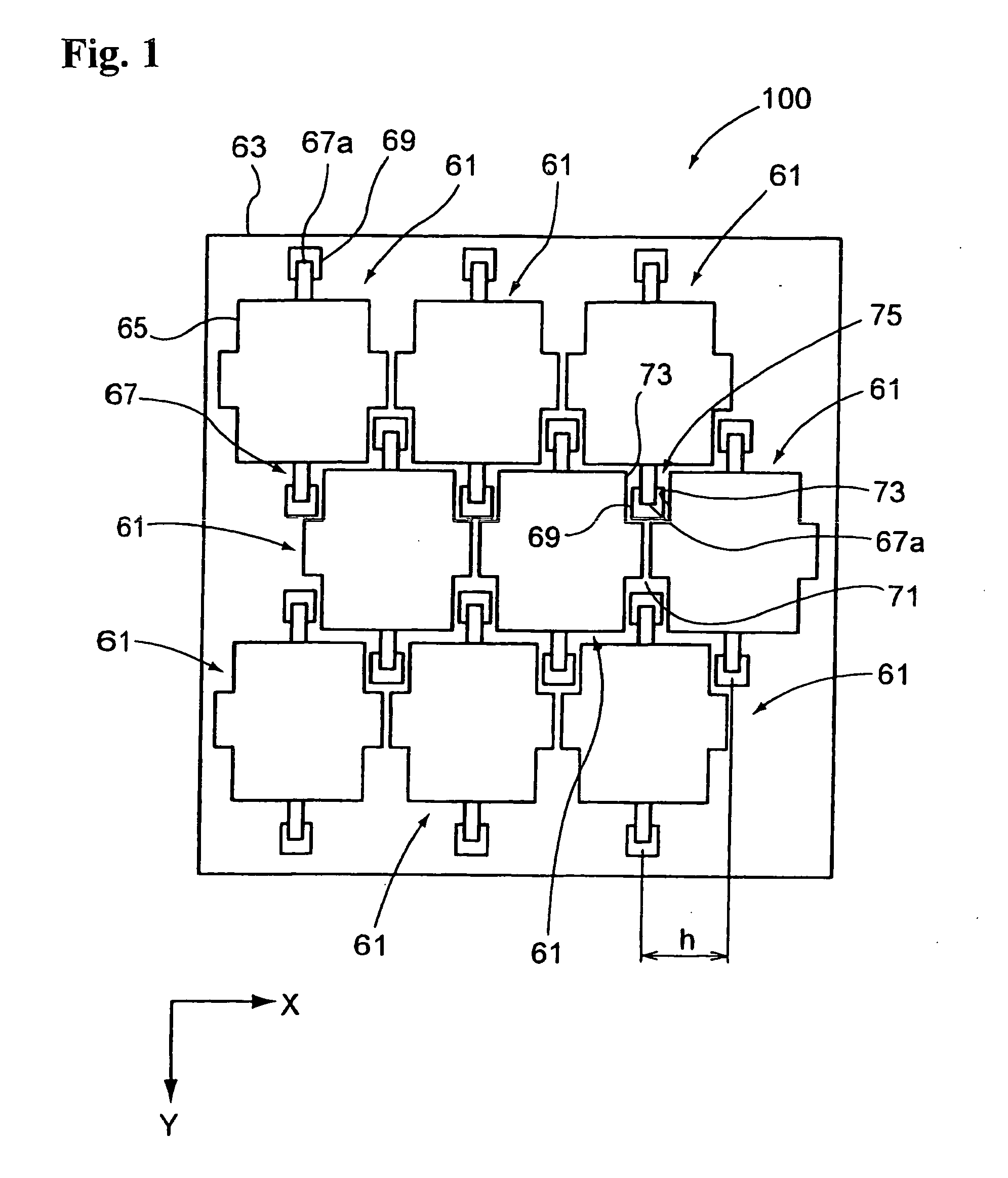
[0056]FIG. 2 is a plan view of the optical modulation element array according to the second embodiment in which a micro mirror is floated and disposed by a supporting portion for micro mirror (supporting portion for optical function film). FIGS. 3A and 3B are schematic drawings, FIG. 3A explaining a sectional view along line B-B in FIG. 2, FIG. 3B explaining a sectional view along line C-C in FIG. 2. In this embodiment, the same reference character is given to the same member as in FIG. 1, and overlapping description thereof is omitted.

[0057] The optical modulation element array 200 includes an array of optical modulation elements 81. The optical modulation element 81 includes a micro mirror 83 provided above a substrate 63 (see FIGS. 3A and 3B), a hinge 67 supporting the micro mirror 83 so that the micro mirror 83 can be tilted, and a first support 69 by which an end 67a of the hinge 67 ...

third embodiment

[0078] Next, the optical modulation element array according to an aspect of the invention will be described.

[0079]FIG. 5 is a plan view of the optical modulation element array according to the third embodiment in which a movable film is provided. FIGS. 6A to 6C are schematic explanatory drawings, FIG. 6A being a sectional view along line D-D in FIG. 5, FIG. 6B being a sectional view along line E-E in FIG. 5, FIG. 6C being a sectional view along line F-F in FIG. 5. In this embodiment, the same reference character is given to the same member as in FIGS. 1 and 2, and overlapping description thereof is omitted.

[0080] The optical modulation element array 300 includes an array of optical modulation elements 111. The optical modulation element 111 includes a micro mirror 83 provided above a substrate 63 (see FIGS. 6A to 6C, a hinge 67 supporting the micro mirror 83 so that the micro mirror 83 can be tilted, a first support 69 by which an end 67a of the hinge 67 is connected to the substra...


PUM


Abstract

An optical modulation element array includes: a substrate and optical modulation elements two-dimensionally arranged in a first direction and a second direction, the first direction being perpendicular to the second direction, and at least a portion of the end of the hinge is disposed in a gap between optical modulation elements next to each other in the first direction, the optical modulation elements next to each other in the first direction is located next to the optical modulation elements having the end of the hinge, in the second direction.

Description

BACKGROUND OF THE INVENTION [0001] 1. Field of the Invention [0002] The invention relates to an optical modulation element array mounted on various optical apparatuses, e.g., an on-demand digital exposure apparatus used in a photolithography process, an image forming apparatus, such as a digital exposure printer, a projection display apparatus, such as a projector, or a micro display apparatus, such as a head-mounted display. More particularly, the invention relates to an optical modulation element array in which an optical modulation element of rotational displacement type is arranged one-dimensionally or two-dimensionally by the MEMS (Micro Electro Mechanical Systems) technology. [0003] 2. Background Art [0004] Liquid crystal elements, elements using electro-optic crystal or magneto-optic crystal, or optical modulation elements according to the MEMS technology are known as optical modulation elements mounted on an optical apparatus, e.g., an on-demand digital exposure apparatus us...

Claims


Application Information

Patent Timeline
Patent Type & Authority Applications(United States)
IPC IPC(8): G02B26/00
CPCG02B26/0841
Inventor KIMURA, KOICHIOGIKUBO, SHINYA
Owner FUJIFILM CORP
Why Eureka
Try Eureka