Element arrangement check device and printed circuit board design system

a technology of element placement and design system, which is applied in the direction of computer aided design, program control, instruments, etc., can solve the problems of serving as a source of radiation noise, and achieve the effects of reducing radiation noise, high degree of completeness, and easy access to high frequency components

Inactive Publication Date: 2006-12-21
GK BRIDGE 1
View PDF4 Cites 13 Cited by
  • Summary
  • Abstract
  • Description
  • Claims
  • Application Information

AI Technical Summary

Benefits of technology

[0012] An element placement check system pertaining to the invention with the construction can determine whether or not a positional relationship capable of removing a high frequency component with ease is established by checking the positional relationship such as a connection sequence of a power supply decoupling element and a power supply via hole based on the first wire length between the power supply terminal of the integrated circuit and the power supply decoupling element and the second wire length between the power supply terminal and the power supply via hole.
[0013] According to an element placement check system and a printed wiring board design system pertaining to the invention, it can be checked whether or not a connection sequence effective for reduction in radiation noise of a printed wiring board is established, thereby enabling a printed wiring board with a high degree of completeness to be designed from the viewpoint of EMC (Electromagnetic Compatibility).

Problems solved by technology

That is, if a placement position of a bypass capacitor is inappropriate, high frequency energy from the power supply terminal is not removed sufficiently and spreads all over the power supply plane, leading to a possibility of serving as a source of radiation noise.

Method used


Image

  • Element arrangement check device and printed circuit board design system
  • Element arrangement check device and printed circuit board design system
  • Element arrangement check device and printed circuit board design system

Examples


first embodiment

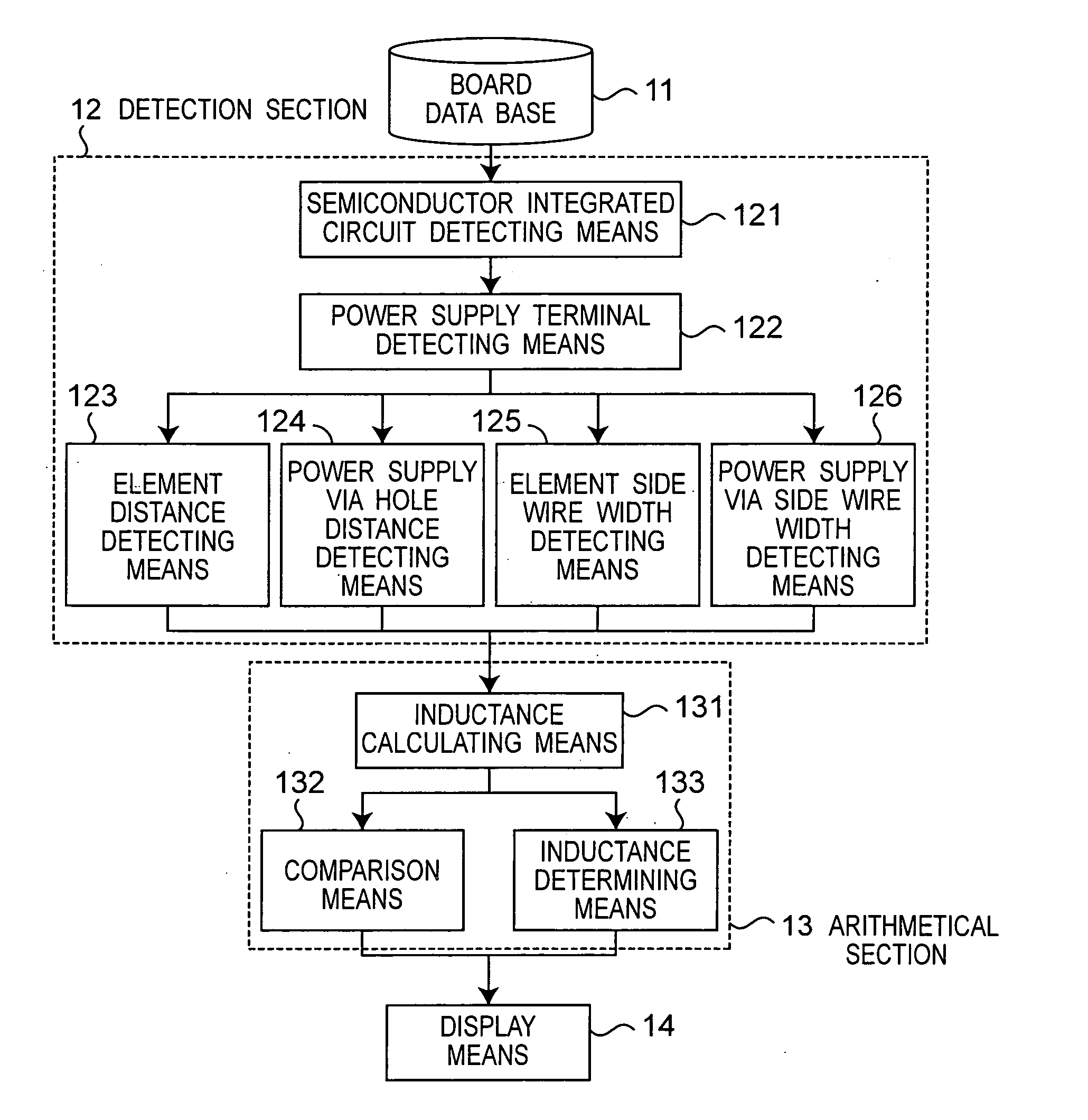
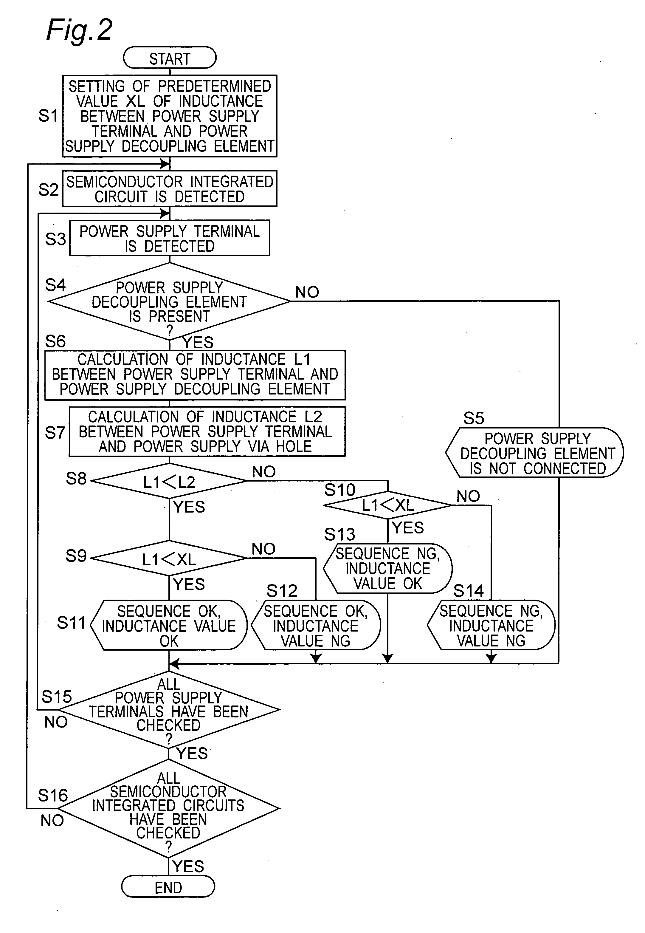
[0036] An element placement check system of a first embodiment pertaining to the invention has a wiring pattern for mounting an integrated circuit and a power supply decoupling element and the like connected to a power supply terminal of the integrated circuit on a mounting surface, wherein in printed wiring board design that the wiring pattern is connected to a power supply plane for providing the power supply through a power supply via hole, it can check whether or not there has been established placement and the wiring pattern of elements such as the power supply terminal of the integrated circuit, the power supply decoupling element and the power supply via hole effectively bypasses a high frequency component with the help of the power supply decoupling element to thereby enable a through current to be effectively prevented.

[0037] Note that an element placement check system for a printed wiring board pertaining to the invention can also check element placement on a multilayer p...

second embodiment

[0086] Then, further description will be given of the processing in the second embodiment using a simplified processing in the first embodiment with reference to a flowchart shown in FIG. 4.

[0087] To be concrete, the second embodiment has a step S61 of detecting the distance (D1), which is the length of the wire, from a power supply terminal to a power supply decoupling element instead of step S6 of calculating the inductance value L1 of the wire between the power supply terminal and the power supply decoupling element based on the distance (D1), which is the length of the wire from the power supply terminal to the power supply decoupling element and width W1 of the wire, and further has step S71 of detecting the distance (D2), which is the length of the wire from the power supply terminal to the power supply via hole instead of step S7 of calculating the inductance value L2 of the wire between the power supply terminal and the power supply via hole.

[0088] In step S81 instead of s...

third embodiment

[0127] Description will be given of a printed wiring board element placement check processing method of the third embodiment of the invention based on a flowchart shown in FIG. 12.

[0128] The printed wiring board element placement check processing method of the third embodiment, in a similar way to that in the printed wiring board element placement check processing method of the second embodiment, checks a connection sequence based on the distance (D1), which is the length of the wire from the power supply terminal to the power supply decoupling element and the distance (D2), which is the length of the wire from the power supply terminal to the power supply via hole and the third embodiment is different from the second embodiment in that a predetermined value is given to the distance from the power supply terminal to the power supply decoupling element and a distance is checked simultaneously in addition to a connection sequence.

[0129] To be concrete, added in the process are: step...


PUM


Abstract

An element placement check system for checking element placement on a printed wiring board having wiring by which a power supply terminal of an integrated circuit and a power supply decoupling element for the power supply terminal are connected on a mounting surface on which the integrated circuit is mounted, wherein the wiring is connected to a power supply plane for providing a direct current power supply to the power supply terminal through a power supply via hole, including: element distance detecting means detecting a first wire length between the power supply decoupling element and the power supply terminal; power supply via hole distance detecting means detecting a second wire length between the power supply via hole and the power supply terminal; and determination means determining a positional relationship of the power supply decoupling element and the power supply via hole to the power supply terminal based on the first and second wire lengths, thereby providing a check system and a printed wiring board design system capable of checking a connection sequence of a power supply decoupling element such as a bypass capacitor and the power supply via hole connected to the power supply plane feeding a direct current power supply to the power supply terminal as viewed from the power supply terminal of an integrated circuit.

Description

TECHNICAL FIELD [0001] This invention relates to an element placement check system for a printed wiring board and a printed wiring board design system, and particularly, an element placement check system for a bypass capacitor placed in the neighborhood of a power supply terminal of an integrated circuit. BACKGROUND ART [0002] On a printed wiring board having high speed integrated circuits thereon, bypass capacitors have been usually placed in the neighborhoods of power supply terminals of each of the integrated circuits. [0003] It has been generally known that a bypass capacitor plays a role to cause a through current generated at a power supply terminal when a high speed integrated circuit is switched to flow back to ground in the neighborhood of the power supply terminal to thereby prevent propagation of high frequency energy (a high frequency component) onto the power supply plane and a role to provide a direct current power supply to the integrated circuit. [0004] That is, if a...

Claims


Application Information

Patent Timeline
Patent Type & Authority Applications(United States)
IPC IPC(8): G06F17/50
CPCG06F17/5081G06F17/5036G06F30/398G06F30/367
Inventor HAMADA, SEIJIFUSAYASU, HIROTSUGUMIMURA, SHOICHIIRIKIIN, MIYOKO
Owner GK BRIDGE 1
Why Eureka
Try Eureka