
Pre-patterned thin film capacitor and method for embedding same in a package substrate

a technology of pre-patterned thin film capacitors and substrates, applied in the field of semi-conductor packaging, can solve the problems of limiting the operational capabilities of passive components, substrate scalability, and the use of this integration scheme is not without problems

Inactive Publication Date: 2006-12-28
INTEL CORP
View PDF28 Cites 33 Cited by
  • Summary
  • Abstract
  • Description
  • Claims
  • Application Information

AI Technical Summary

Problems solved by technology

Restricting the location of the passive components to the substrate's surface however can limit the passive components' operational capabilities (due to their inherent distance from the semiconductor device) and the substrate's scalability.
The use of this integration scheme however is not without its problems.

Method used


Image

  • Pre-patterned thin film capacitor and method for embedding same in a package substrate
  • Pre-patterned thin film capacitor and method for embedding same in a package substrate
  • Pre-patterned thin film capacitor and method for embedding same in a package substrate

Examples


Embodiment Construction

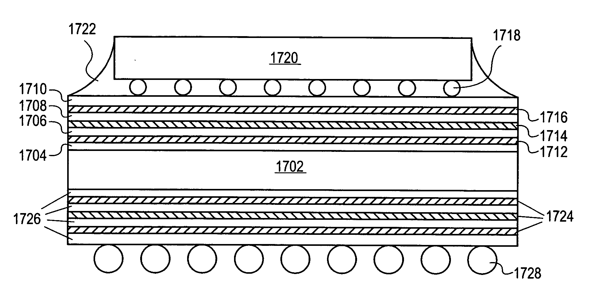
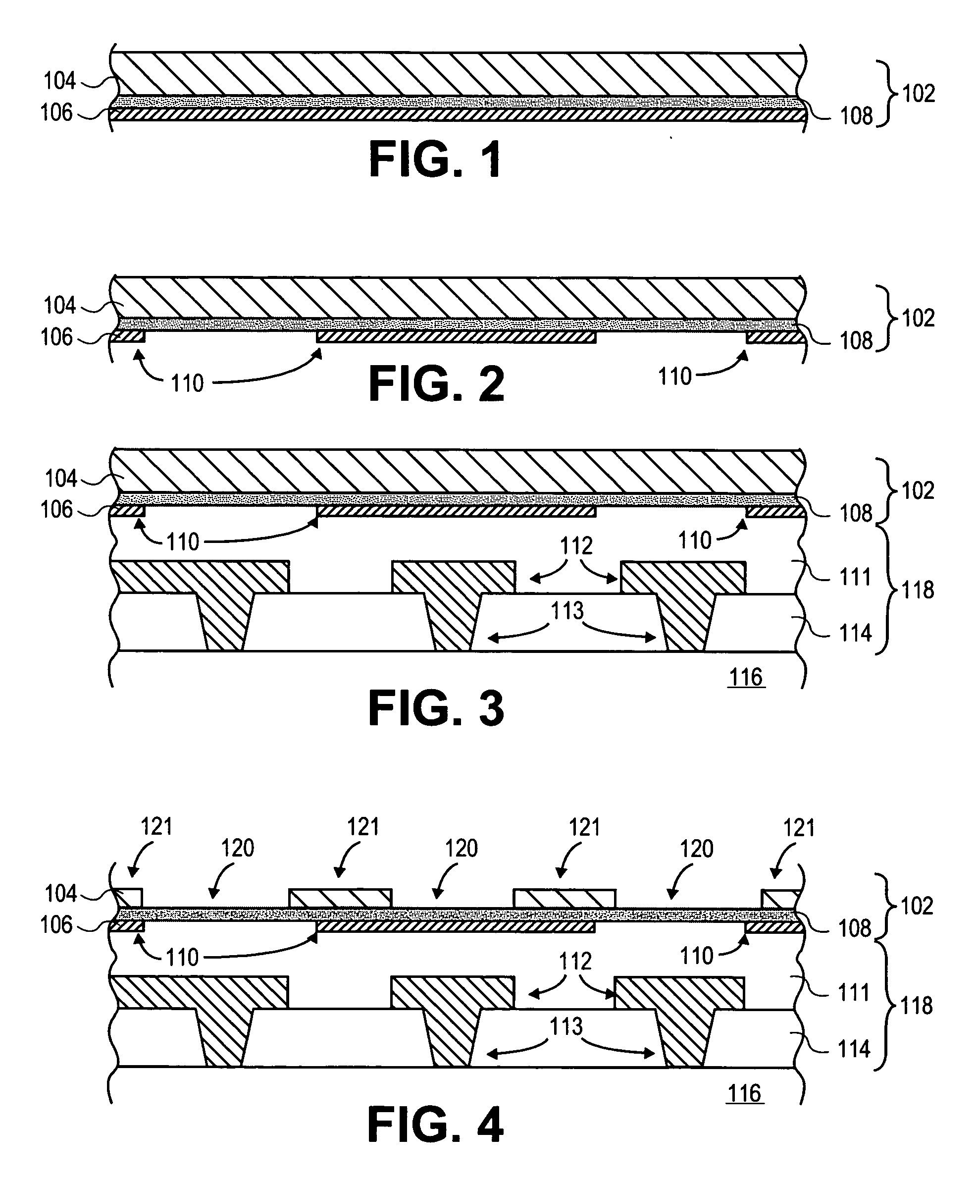
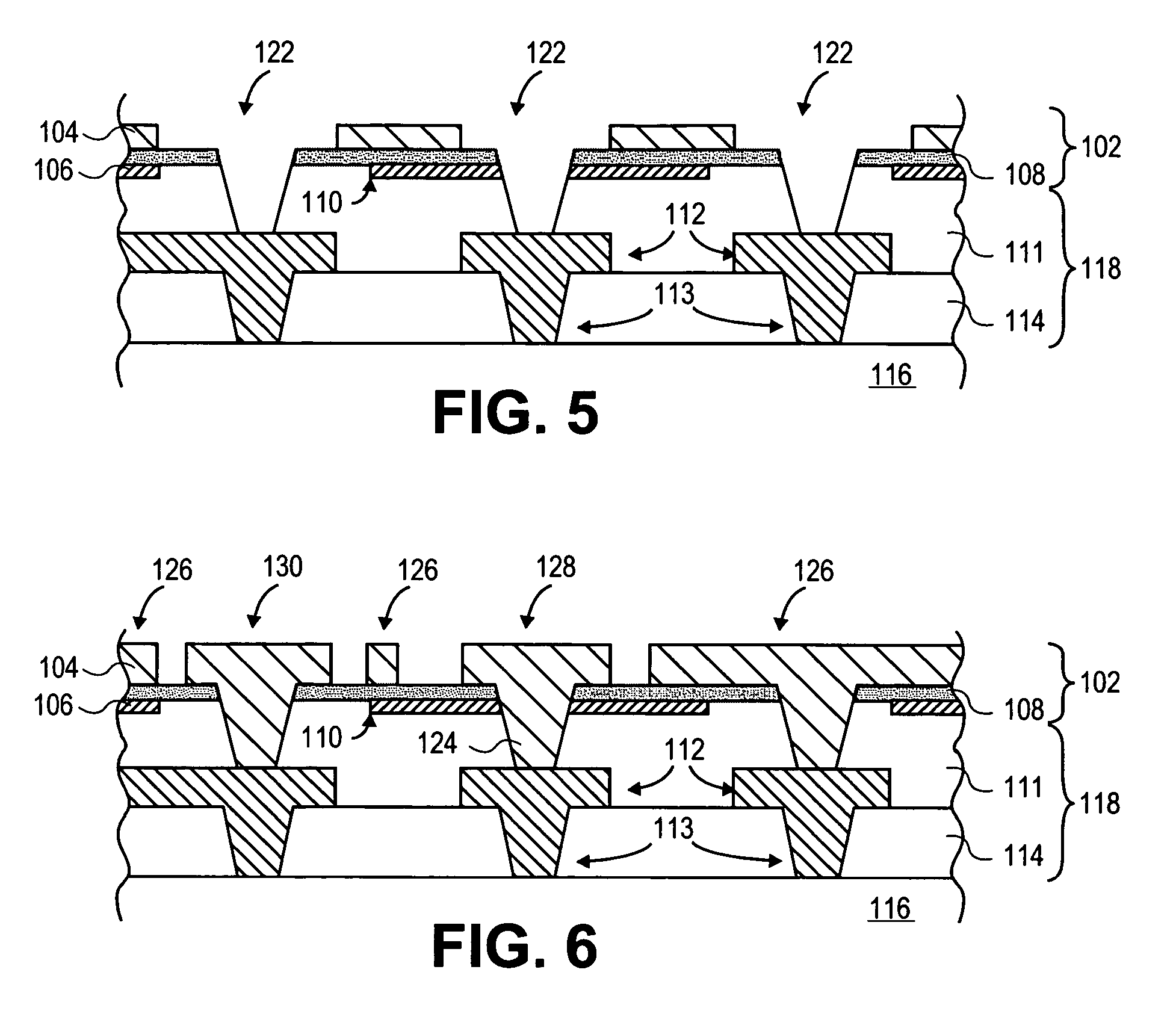
[0010] In the following detailed description, an embedded passive structure and its method of formation are disclosed. Reference is made to the accompanying drawings within which are shown, by way of illustration, specific embodiments by which the present invention may be practiced. It is to be understood that other embodiments may exist and that other structural changes may be made without departing from the scope and spirit of the present invention.

[0011] The terms on, above, below, and adjacent as used herein refer to the position of one layer or element relative to other layers or elements. As such, a first element disposed on, above, or below a second element may be directly in contact with the second element or it may include one or more intervening elements. In addition, a first element disposed next to or adjacent a second element may be directly in contact with the second element or it may include one or more intervening elements.

[0012] In one embodiment, a thin film lami...


PUM

PropertyMeasurementUnit
Temperatureaaaaaaaaaa
Dielectric polarization enthalpyaaaaaaaaaa
Electrical conductoraaaaaaaaaa

Abstract

An embedded passive structure, its method of formation, and its intergration onto a substrate during fabrication are disclosed, In one embodiment the embedded passive structure is a thin film capacitor (TFC) formed using a thin film laminate that has been mounted onto a substrate. The TFC's capacitor dielectric and / or lower electrode layers are patterned in such a way as to reduce damage and improve cycle time. In one embodiment, the capacitor dielectric has a high dielectric constant and the substrate is an organic packaging substrate.

Description

FIELD OF THE INVENTION [0001] Embodiments of the present invention relate generally to semiconductor technology and more specifically to semiconductor packaging. BACKGROUND OF THE INVENTION [0002] The demand for increased mobility in consumer electronics is pressuring manufacturers to scale electronic technologies (e.g., semiconductor devices) to ever smaller dimensions. At the same time, the demand for increased functionality, speed, noise elimination, etc., is forcing manufactures to increase the number of passive components (e.g., capacitors and resistors) used by consumer electronic devices. Passive component integration has traditionally been accomplished by mounting them onto package and / or printed circuit board (PCB) substrate surfaces. Restricting the location of the passive components to the substrate's surface however can limit the passive components' operational capabilities (due to their inherent distance from the semiconductor device) and the substrate's scalability. [0...

Claims


Application Information

Patent Timeline
IPC IPC(8): H01L23/02
CPCH01G4/228Y10T29/417H01L23/49822H01L2924/12044H05K1/162H05K3/048H05K3/4652H05K2201/0175H05K2201/0179H05K2201/0355H05K2201/09763H01L2224/16225H01L2224/32225H01L2224/73204H01L2924/15311H01G4/33H01L2924/00
Inventor MIN, YONGKI
Owner INTEL CORP
Features
  • Generate Ideas
  • Intellectual Property
  • Life Sciences
  • Materials
  • Tech Scout
  • Unparalleled Data Quality
  • Higher Quality Content
  • 60% Fewer Hallucinations
Learn More