

Electronic circuit, method of driving electronic circuit, electro-optical device, method of driving electro-optical device, and electronic apparatus
- Summary
- Abstract
- Description
- Claims
- Application Information
AI Technical Summary
Benefits of technology
Problems solved by technology
Method used
Image

Examples
first embodiment
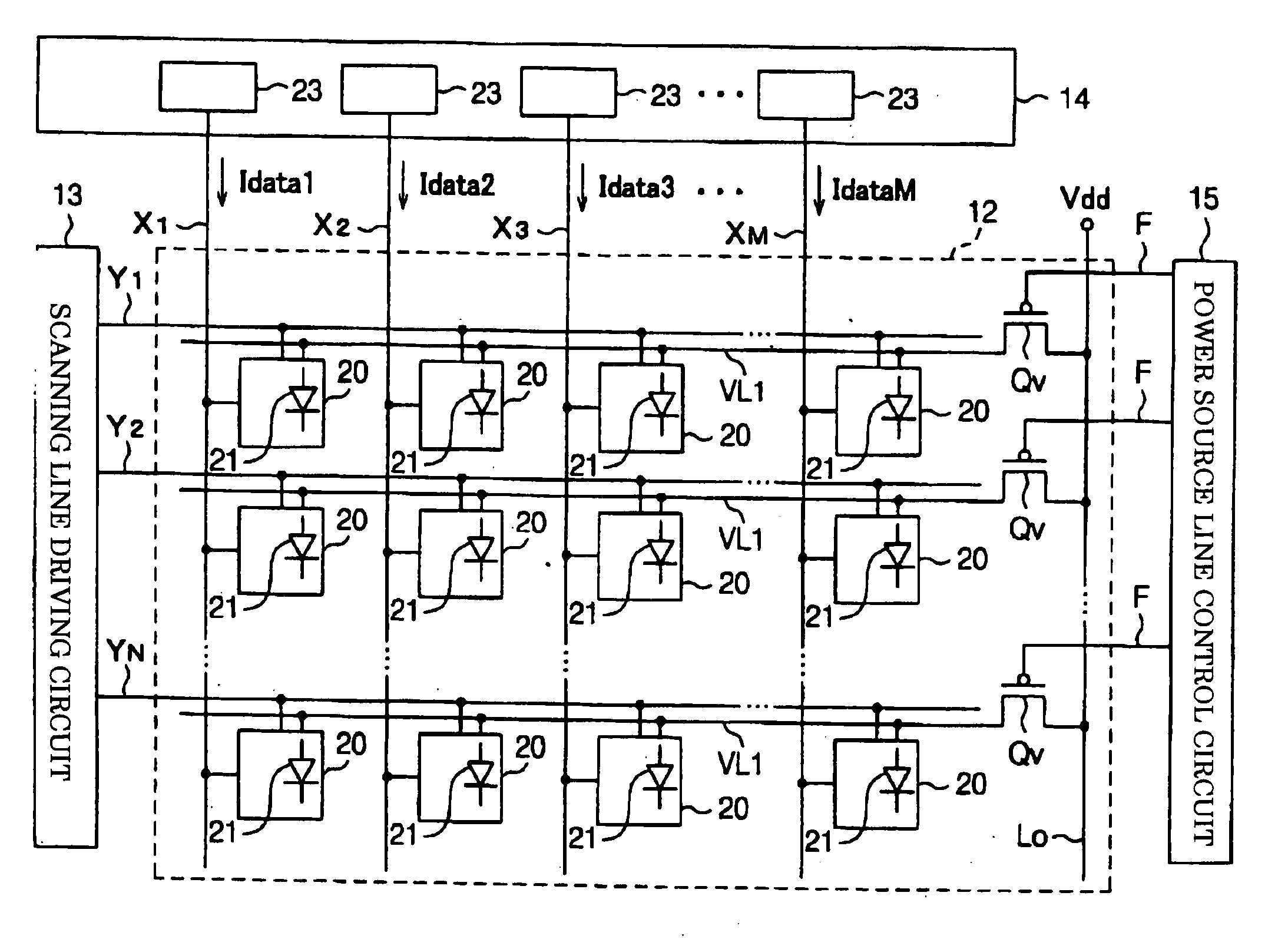
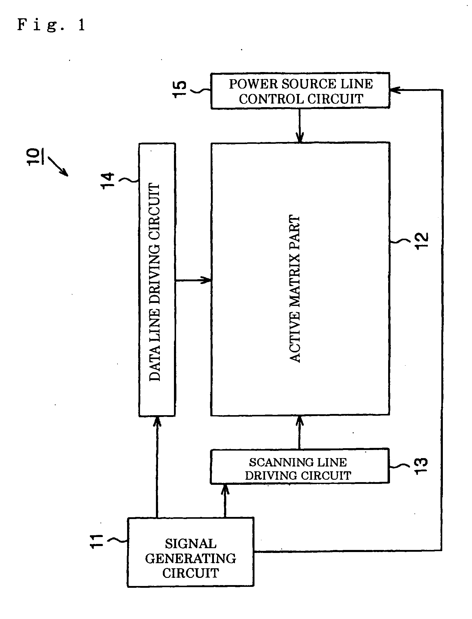
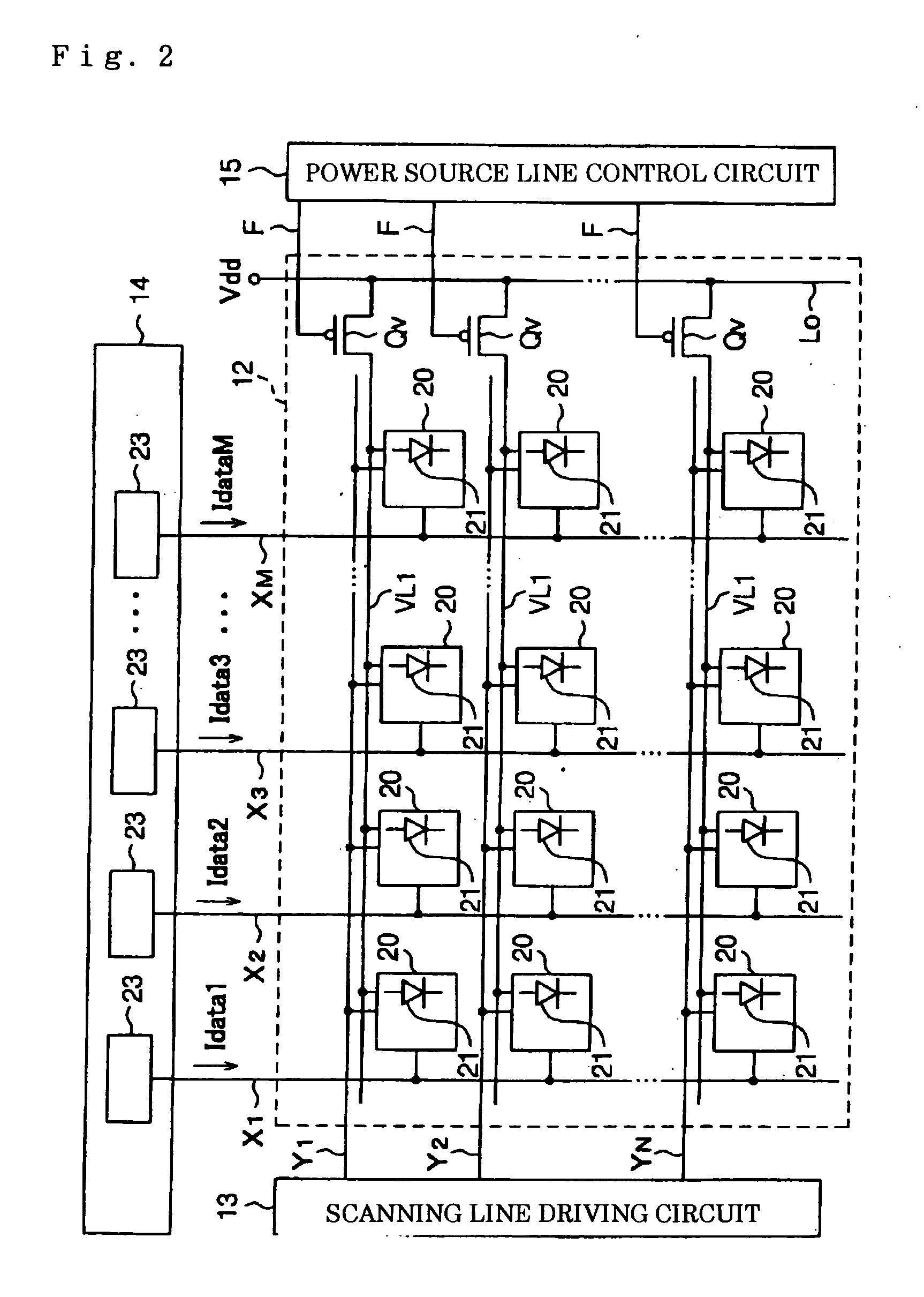
[0055] Now, the present invention will be described with reference to FIGS. 1 to 4. FIG. 1 is an exemplary circuitry block diagram illustrating a circuit configuration of an organic EL display device as an electro-optical device. FIG. 2 is an exemplary circuitry block diagram illustrating a circuit configuration of a display panel part and a data line driving circuit. FIG. 3 is an exemplary circuit diagram of a pixel circuit. FIG. 4 is a timing chart describing a method of driving the pixel circuit.
[0056] An organic EL display device 10 can include a signal generating circuit 11, an active matrix part 12, a scanning line driving circuit 13, a data line driving circuit 14, and a power source line control circuit 15. The signal generating circuit 11, the scanning line driving circuit 13, the data line driving circuit 14, and the power source line control circuit 15 may be constructed using an independent electronic component, respectively. For example, the signal generating circuit 11...
second embodiment
[0087]FIG. 5 is an exemplary circuitry block diagram illustrating a circuit configuration of the active matrix part 12a and the data line driving circuit 14 of the organic EL display device 10 according to the FIG. 6 is an exemplary circuit diagram of pixel circuits 30 arranged in the active matrix part 12a.
[0088] The active matrix part 12 is provided with second power source lines VL2 in parallel to the first power source lines VL1. As shown in FIG. 6, each of the plurality of second power source lines VL2 is connected to the holding capacitor Co of each pixel circuit 30 and connected to the voltage supply line Lo.
[0089] As shown in FIG. 6, each pixel circuit 30 can include the driving transistor Q1, the transistor Q2, the switching transistor Q3, and the holding transistor Co.
[0090] The drain of the driving transistor Q1 is connected to an anode of an organic EL element 21 and the drain of the transistor Q2. A cathode of the organic EL element 21 is connected to ground. The so...
PUM
 Abstract
Description
Claims
Application Information