

High-stability shift circuit using amorphous silicon thin film transistors
a technology shift circuits, applied in static storage, digital storage, instruments, etc., can solve the problems of increasing the number of the complexity of the manufacturing process and the electrical characteristics, and the increase of the tft elements that follow the affection of bias stress, etc., to reduce the shift of threshold voltage, increase the lifetime of amorphous silicon thin film transistors, and increase the operating time
- Summary
- Abstract
- Description
- Claims
- Application Information
AI Technical Summary
Benefits of technology
Problems solved by technology
Method used
Image

Examples
Embodiment Construction
[0024] The detailed descriptions for content and technology of this invention associate with figures are as follows.
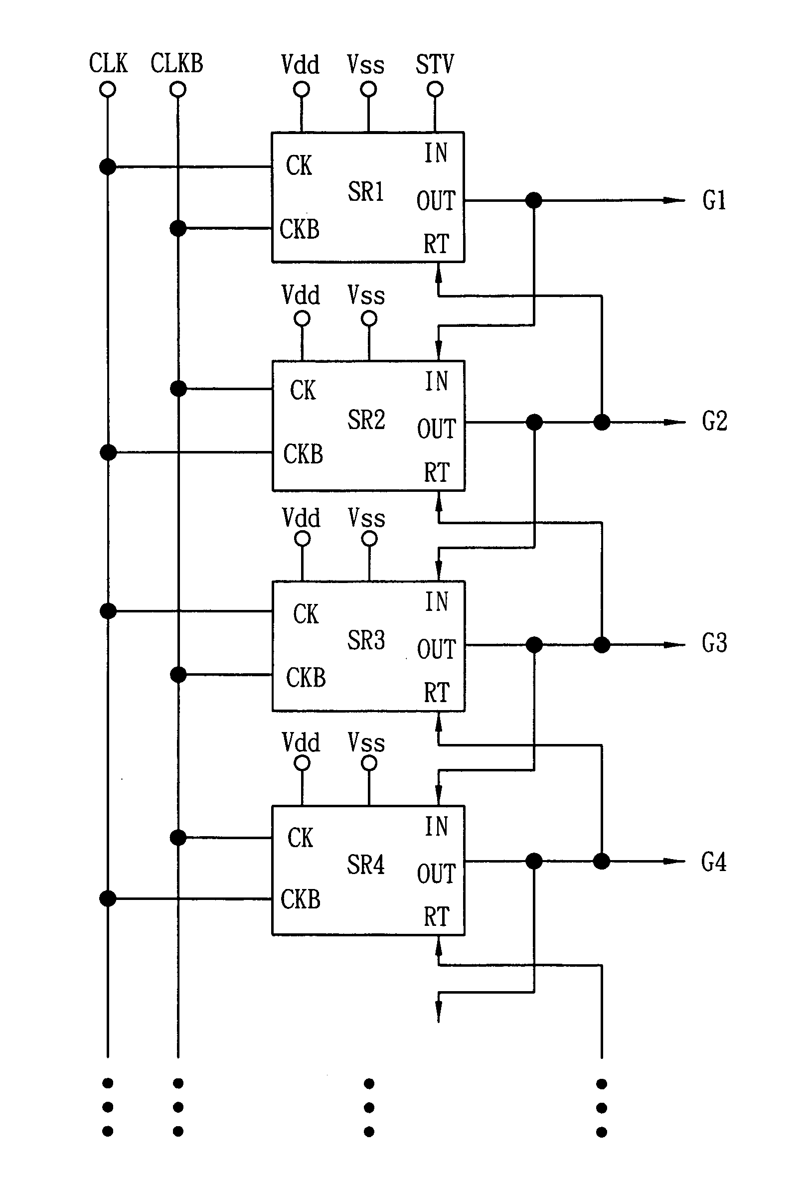
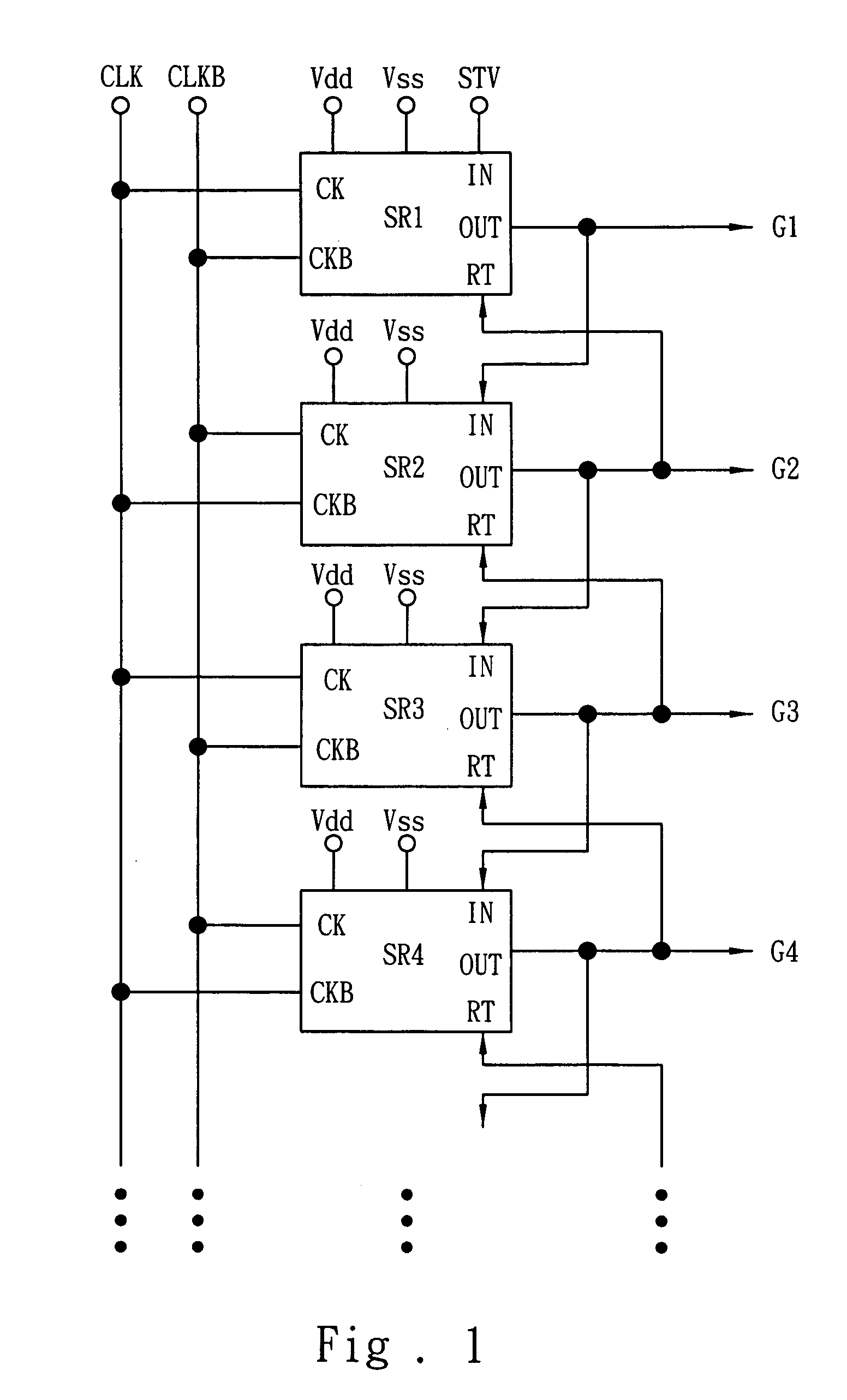
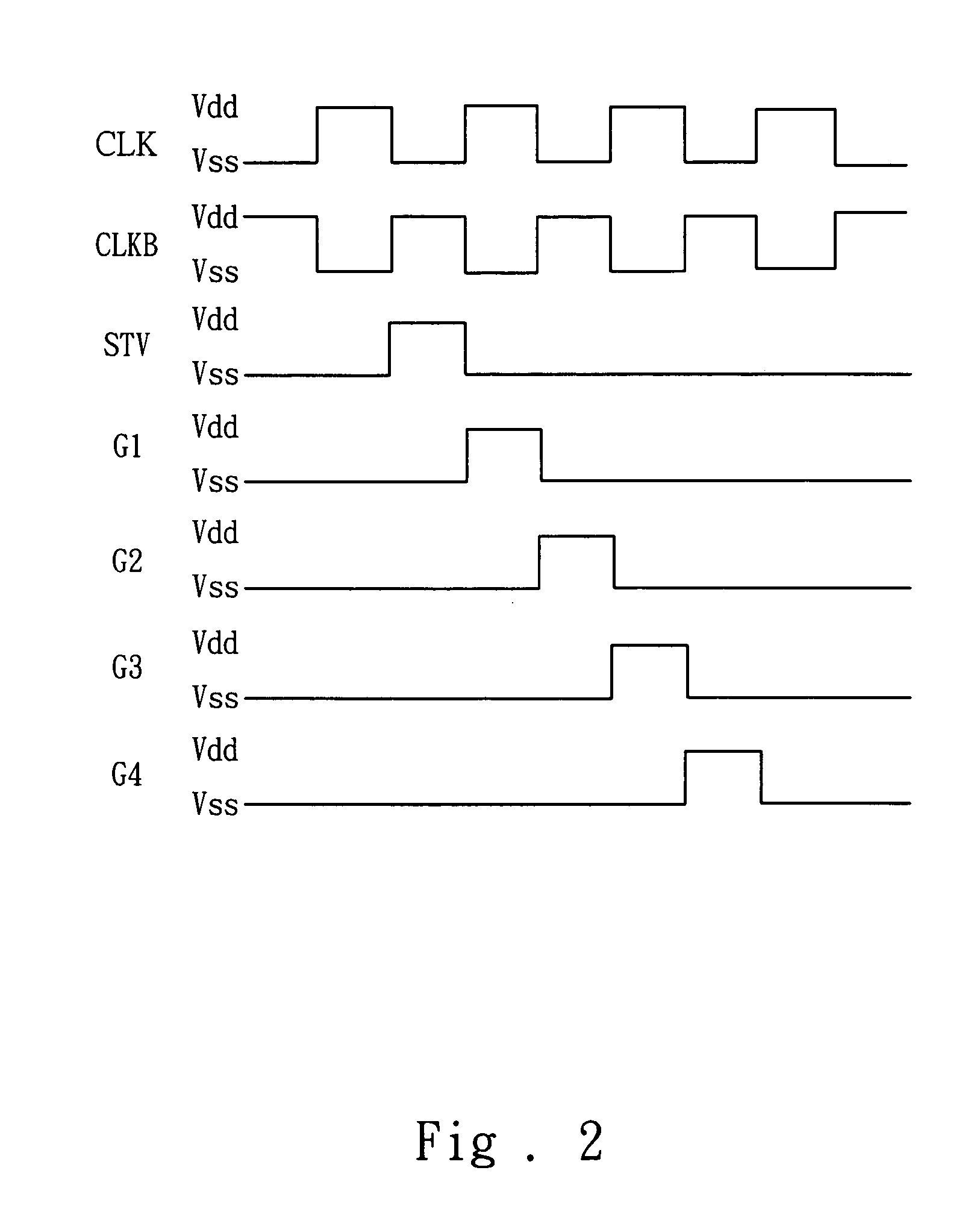
[0025] Please refer to FIGS. 1 and 2, which are the block diagram and the timing diagram for the output and input signals, respectively, for the shift register of the current invention. As shown in the figures, the present invention is applied to shift register circuits that are composed of amorphous silicon thin film transistors. The invention is a scanning driving circuit that can be integrated to a glass substrate. The shift register of this invention is composed of several stages. The stages are connected in serial and send the output signals G1, G2, G3, G4, . . . to the gate lines in the panel. The two power sources are a high-level supply voltage Vdd and a low-level supply voltage Vss. The input signals include the first clock-pulse signal CLK and the second clock-pulse signal CLKB, they are out-of-phase to each other, and the start signal STV.
[0026] Initially,...
PUM
 Abstract
Description
Claims
Application Information