Capacitor with nano-composite dielectric layer and method for fabricating the same

Active Publication Date: 2007-01-04
SK HYNIX INC
View PDF11 Cites 19 Cited by
  • Summary
  • Abstract
  • Description
  • Claims
  • Application Information

AI Technical Summary

Benefits of technology

[0011] It is, therefore, an object of the present invention to provide a capacitor with a nano-composite dielectric layer with an effecti

Problems solved by technology

However, even though the cell sizes have been decreased, a certain level of capacitance is often required to prevent a soft error event and shorten a refresh time.
However, Ta2O5 has a poor leakage current characteristic.
Although Al2O3 whose dielectric constant is 9 has a good leakage current characteristic, it is still limited to secure a desired level of capacitance due to a low dielectric constant value.
Thus, HfO2 is prone to an electric shock, thereby decreasing durability of the capacitor.
However, it is often difficult to apply Al2O3 to a concave type capacitor in

Method used


Image

  • Capacitor with nano-composite dielectric layer and method for fabricating the same
  • Capacitor with nano-composite dielectric layer and method for fabricating the same
  • Capacitor with nano-composite dielectric layer and method for fabricating the same

Examples


Embodiment Construction

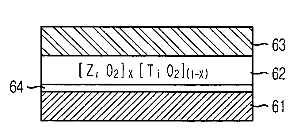
[0022] A capacitor with a nano-composite dielectric layer and a method for fabricating the same in accordance with exemplary embodiments of the present invention will be described in detail with reference to the accompanying drawings.

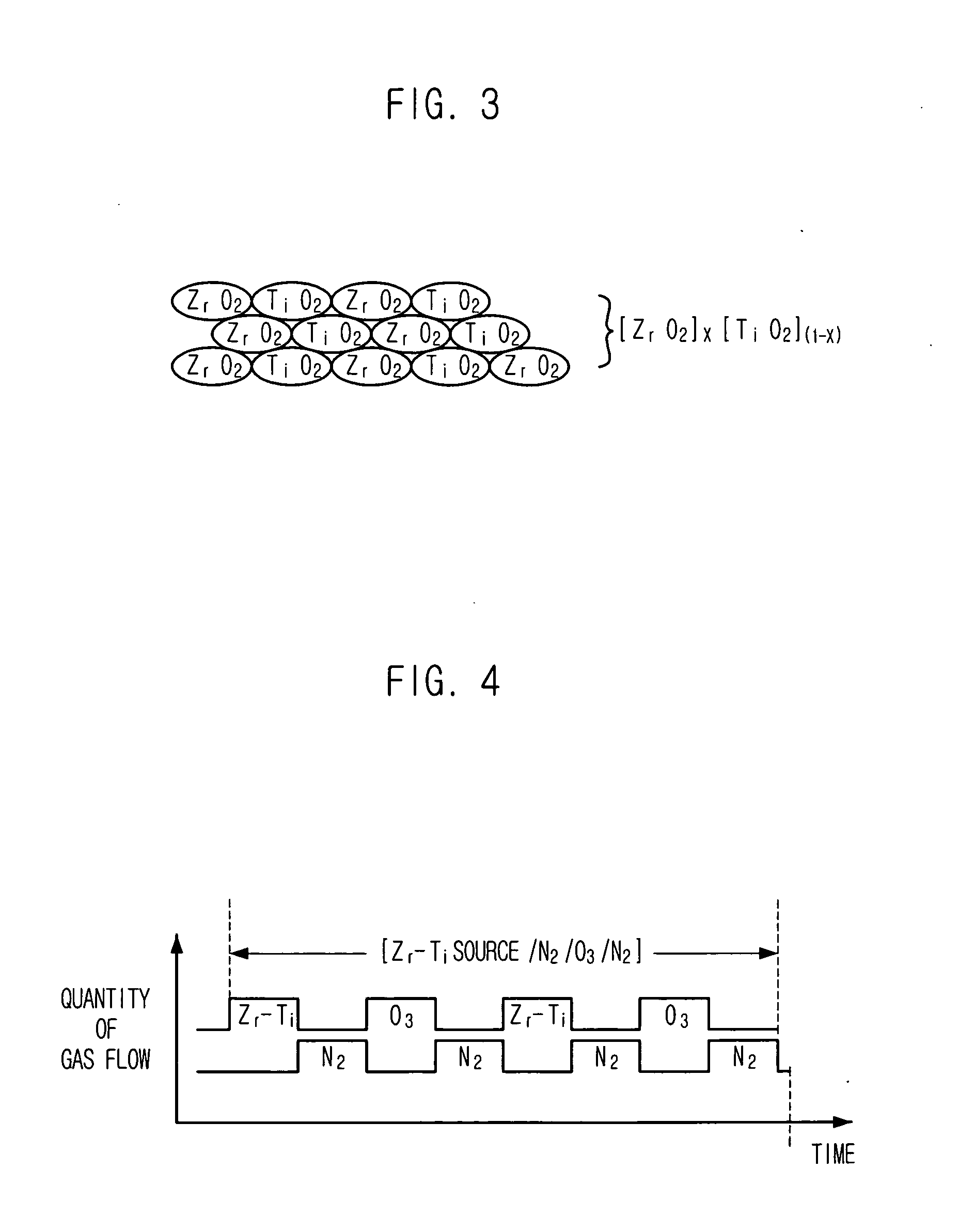
[0023] According to an exemplary embodiment of the present invention, a [ZrO2]x[TiO2](1-x) dielectric layer, which is used as a dielectric layer of a capacitor, is introduced. The [ZrO2]x[TiO2](1-x) dielectric layer is obtained by mixing a zirconium oxide (ZrO2) layer with a titanium oxide (TiO2) layer in a predetermined ratio. ZrO2 has high band gap energy (Eg), and TiO2 has a high dielectric constant (ε). Herein, the [ZrO2]x[TiO2](1-x) layer is a nano-composite dielectric layer.

[0024] Table 1 below shows dielectric constants, band gap energy values and conduction band offset (CBO) values depending on dielectric material types.

TABLE 1DielectricDielectricBand Gap EnergyCBO to SiMaterialConstant(Eg, eV)(eV)SiO23.98.93.5Si3N475.12.4Al2O398.72.8Y2O3155...


PUM

PropertyMeasurementUnit
Temperatureaaaaaaaaaa

Abstract

A capacitor with a nano-composite dielectric layer and a method for fabricating the same are provided. A dielectric layer of a capacitor includes a nano-composite layer formed by mixing X number of different sub-layers, X being a positive integer greater than approximately 1. A method for forming a dielectric layer of a capacitor includes: forming a nano-composite layer by mixing X number of different sub-layers in the form of a nano-composition, X being a positive integer greater than approximately 1; and densifying the nano-composite layer.

Description

FIELD OF THE INVENTION [0001] The present invention relates to a semiconductor device and a method for fabricating the same; and, more particularly, to a capacitor with a nano-composite dielectric layer and a method for fabricating the same. DESCRIPTION OF RELATED ARTS [0002] As the integration scale of memory products has been accelerated by micronization in semiconductor technology, sizes of unit cells have been rapidly scaled down and a low operation voltage can be achieved. However, even though the cell sizes have been decreased, a certain level of capacitance is often required to prevent a soft error event and shorten a refresh time. Therefore, even though a three-dimensional storage node having a semispherical electrode surface with the large surface area has been implemented, the height of an NO capacitor for use in a dynamic random access memory (DRAM) using a silicon nitride (Si3N4) layer has been continuously increased. The silicon nitride layer is generally formed using d...

Claims


Application Information

Patent Timeline
IPC IPC(8): H01L29/94H01L29/00
CPCH01G4/12H01G4/1218H01G4/1236Y10S977/70H01G4/206Y10S977/902H01L28/40B82Y10/00H10B99/00
Inventor KIL, DEOK-SINHONG, KWONYEOM, SEUNG-JIN
Owner SK HYNIX INC
Why Eureka
Try Eureka