Clock and data recovery circuit and method thereof

a clock and data recovery circuit technology, applied in the direction of digital transmission, pulse automatic control, electrical apparatus, etc., can solve the problems of difficult regulation and optimization of clock and data recovery circuit i, difficult to raise efficiency, and costly for clock and data recovery circuit b, etc., to achieve easy regulation and optimization, and difficult to raise efficiency

Active Publication Date: 2007-01-04
VIA TECH INC
View PDF11 Cites 99 Cited by
  • Summary
  • Abstract
  • Description
  • Claims
  • Application Information

AI Technical Summary

Benefits of technology

[0009] In addition, the current I flowing through the single control path in the above-mentioned architecture simultaneously influences the proportional gain and the integration gain. Thus, the current I, the resistance R related to the resistor 131 and the capacitance C related to the capacitor 132 are not easy to adjust and design. The clock and data recovery circuit I is not easy to regulate and optimize, and its efficiency is hard to raise. Consequently, it is an important subject of the invention to provide a clock and data recovery circuit to solve the above-mentioned problems.
[0010] The invention provides a clock and data recovery circuit including parallel control paths separated from each other and a method thereof.
[0011] The invention discloses a clock and data recovery circuit having parallel dual path. The clock and data recovery circuit includes a phase detecting circuit, a first charge pump, a proportional load circuit, a second charge pump, an integration load circuit, and a voltage control oscillating circuit. The phase detecting circuit respectively compares a phase difference between a data signal and a plurality of clock signals to generate two proportional control signals and two integration control signals for respectively controlling the first charge pump and the second charge pump to generate a first current and a second current. The proportional load circuit and the integration load circuit respectively receive the first current and the second current to output a proportional voltage and an integration voltage. The voltage control oscillating circuit adjusts the phase and frequency of the plurality of clock signals in response to the proportional voltage and the integration voltage. In addition, the clock signals have the same frequency but different phases, and the frequency of the data signal is a multiple of the frequency of the clock signals.
[0012] The invention also discloses a clock and data recovery method. The method includes the following steps of: comparing a phase difference between a data signal and a plurality of clock signals to generate two proportional control signals and two integration control signals; controlling a first charge pump to generate a first current in response to the two proportional control signals, wherein the first current is injected into a proportional load circuit to output a proportional voltage proportionally; controlling a second charge pump to generate a second current in response to the two integration control signals, wherein the second current is injected into an integration load circuit to output an integration voltage; and adjusting phases and frequency of the clock signals in response to the proportional voltage and the integration voltage, wherein the clock signals have the same frequency but different phases, and the frequency of the data signal is a multiple of the frequency of the clock signals.

Problems solved by technology

However, neither the larger resistance R nor the larger capacitance C is provided, it is costly for the clock and data recovery circuit 1.
The clock and data recovery circuit I is not easy to regulate and optimize, and its efficiency is hard to raise.

Method used


Image

  • Clock and data recovery circuit and method thereof
  • Clock and data recovery circuit and method thereof
  • Clock and data recovery circuit and method thereof

Examples


Embodiment Construction

[0023] The present invention will be apparent from the following detailed description, which proceeds with reference to the accompanying drawings, wherein the same references relate to the same elements.

[0024] The clock and data recovery circuit and the method according to the embodiment of the invention will be described with reference to the accompanying drawings.

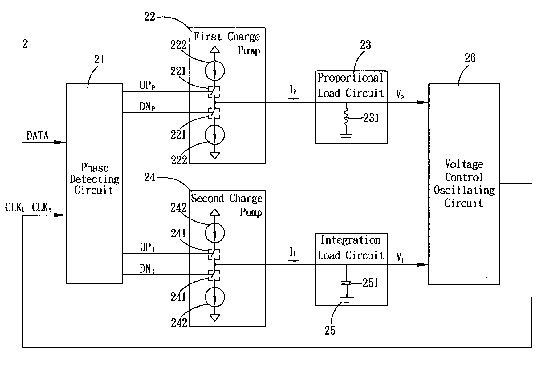
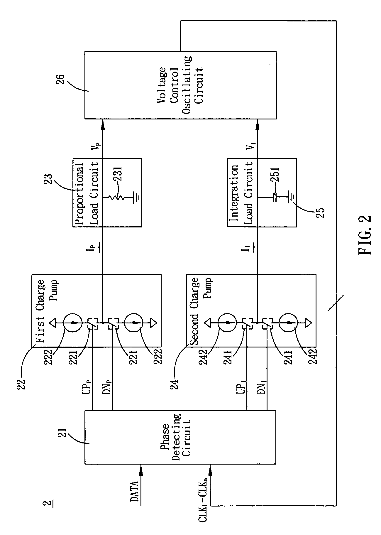
[0025]FIG. 2 is a block diagram showing a clock and data recovery circuit according to an embodiment of the invention. Referring to FIG. 2, the clock and data recovery circuit 2 includes a phase detecting circuit 21, a first charge pump 22, a proportional load circuit 23, a second charge pump 24, an integration load circuit 25 and a voltage control oscillating circuit 26. The phase detecting circuit 21 compares a phase difference between a data signal DATA and a plurality of clock signals CLK1-CLKn to generate two proportional control signals UPP, DNP and two integration control signals UPI, DNI. The clock signals CLK1-...


PUM


Abstract

A clock and data recovery circuit having parallel dual path is disclosed, which includes a phase detecting circuit, a first charge pump, a proportional load circuit, a second charge pump, an integration load circuit, and a voltage control oscillating circuit. The phase detecting circuit respectively compares a phase difference between a data signal and a plurality of clock signals to generate two proportional control signal and two integration control signal for respectively controlling the first charge pump and the second charge pump to generate a first current and a second current. The proportional load circuit and the integration load circuit respectively receive the first current and the second current to output a proportional voltage and an integration voltage. The voltage control oscillating circuit adjusts the phase and frequency of the plurality of clock signals in response to the proportional voltage and the integration voltage.

Description

[0001] This application claims the benefit of U.S. Provisional Application Ser. No. 60 / 695,431, entitled “CLOCK DATA RECOVERY HAVING MULTI-CONTROL PATH”, filed Jul. 1, 2005.BACKGROUND OF THE INVENTION [0002] 1. Field of Invention [0003] The invention relates to a clock and data recovery circuit and a method thereof, and, in particular, to a clock and data recovery circuit including parallel control paths separated from each other and a method thereof. [0004] 2. Related Art [0005] In the modern communication system, high-speed serial signal transmission gradually replaces the conventional parallel signal transmission. During the high-speed sequential signal transmission, the original low-speed parallel signal is converted into a high-speed serial signal to facilitate the transmission. Thus, a clock generating circuit is provided to generating a high-speed clock signal for sampling the high-speed sequential signal. And a clock and data recovery circuit is provided to recover the sampl...

Claims


Application Information

Patent Timeline
Patent Type & Authority Applications(United States)
IPC IPC(8): H03L7/06
CPCH03L7/0893H03L7/091H04L7/033H03L2207/06H03L7/0995
Inventor LIN, JOANNA
Owner VIA TECH INC
Why Eureka
Try Eureka