Wafer dividing method

a technology of dividing method and wafer, which is applied in the direction of semiconductor/solid-state device testing/measurement, manufacturing tools, instruments, etc., can solve the problems of reducing the quality of devices, unable to form uniform deteriorated layers, and the constitution of each device is detected, so as to prevent the formation of the obtained devices from being detected

Active Publication Date: 2007-01-04
DISCO CORP
View PDF4 Cites 9 Cited by
  • Summary
  • Abstract
  • Description
  • Claims
  • Application Information

AI Technical Summary

Benefits of technology

[0007] It is an object of the present invention to provide a wafer dividing method capable of dividing a wafer into individual devices without being influenced by test metal patterns formed on streets and preventing the constitution of the obtained devices from being detected.

Problems solved by technology

That is, when the test metal patterns remain, there is a possibility that the constitution of each device is detected from the metal patterns.
When the TEG is formed on the streets of the wafer, however, there is a problem in that the TEG becomes an obstacle to a laser beam, thereby making it impossible to form a deteriorated layer uniformly.
However, there arises a problem that when the wafer having the deteriorated layers is divided by exerting external force thereto, the TEG is broken like the teeth of a saw, causes contamination and reduces the quality of devices.
Further, there remains the problem that the constitution of devices can be detected from the remaining TEG, resulting in the leakage of a company secret.

Method used


Image

  • Wafer dividing method
  • Wafer dividing method
  • Wafer dividing method

Examples


Embodiment Construction

[0021] Preferred embodiments of the wafer dividing method of the present invention will be described in more detail hereinunder with reference to the accompanying drawings.

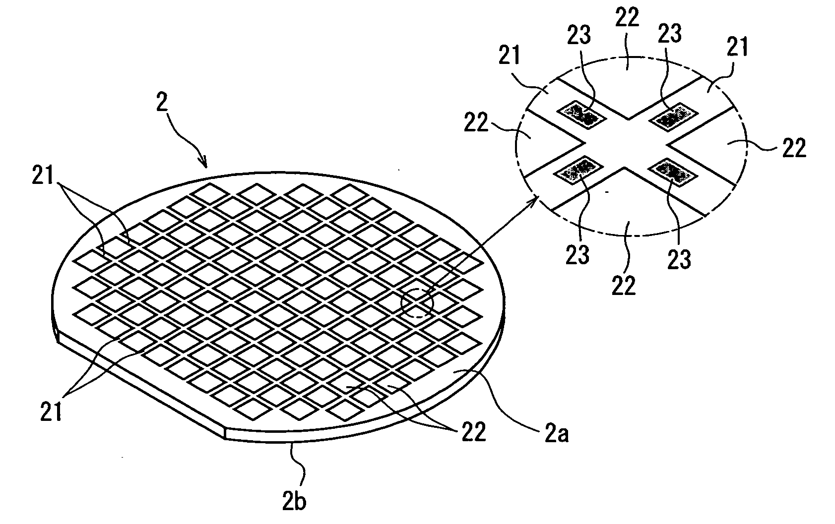
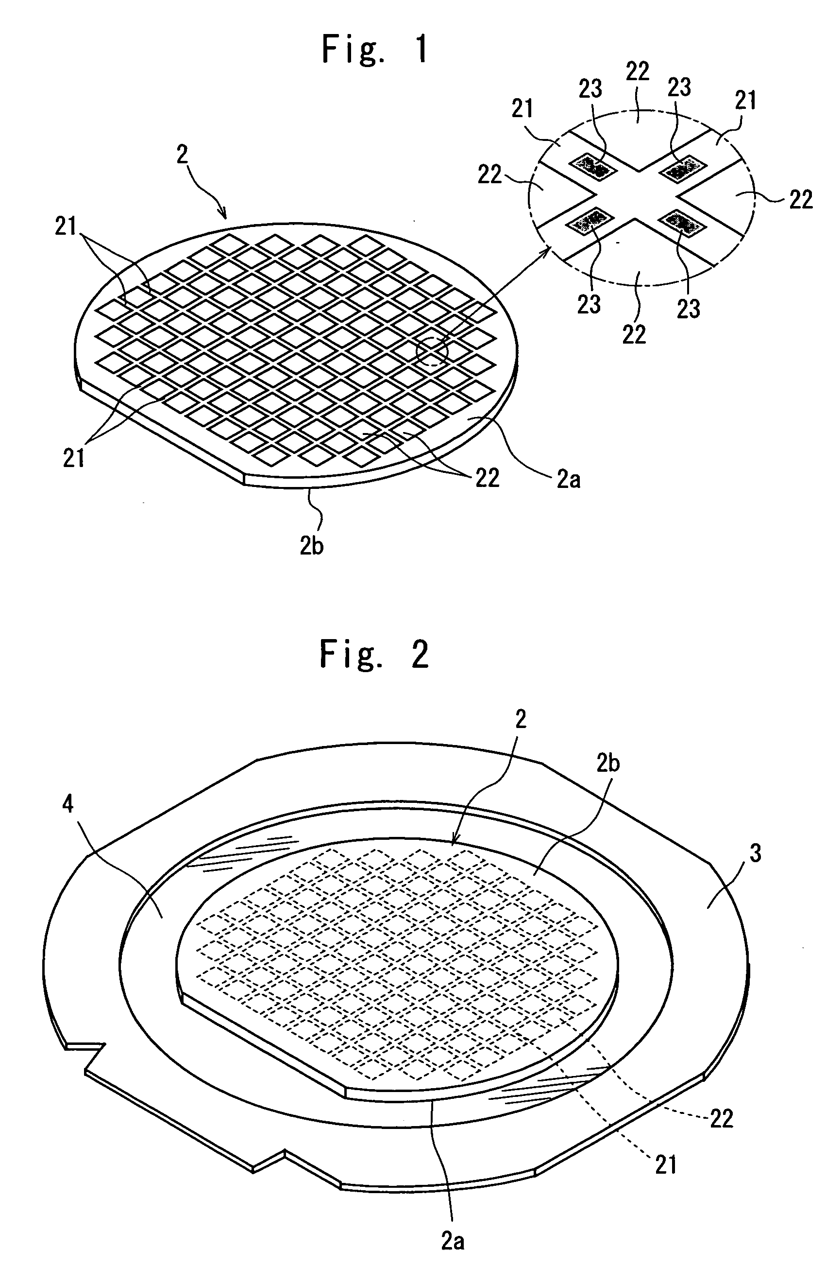
[0022]FIG. 1 is a perspective view of a semiconductor wafer to be divided into individual chips by the wafer dividing method of the present invention. The semiconductor wafer 2 shown in FIG. 1 is a silicon wafer, a plurality of areas are sectioned by a plurality of streets 21 which are arranged in a lattice pattern on the front surface 2a of the semiconductor wafer 2, and a device 22 such as IC or LSI is formed in each of the sectioned areas. A plurality of test metal patterns 23 called “test element group (TEG)” for testing the function of each device 22 are partially formed on the streets 21 of this semiconductor wafer 2.

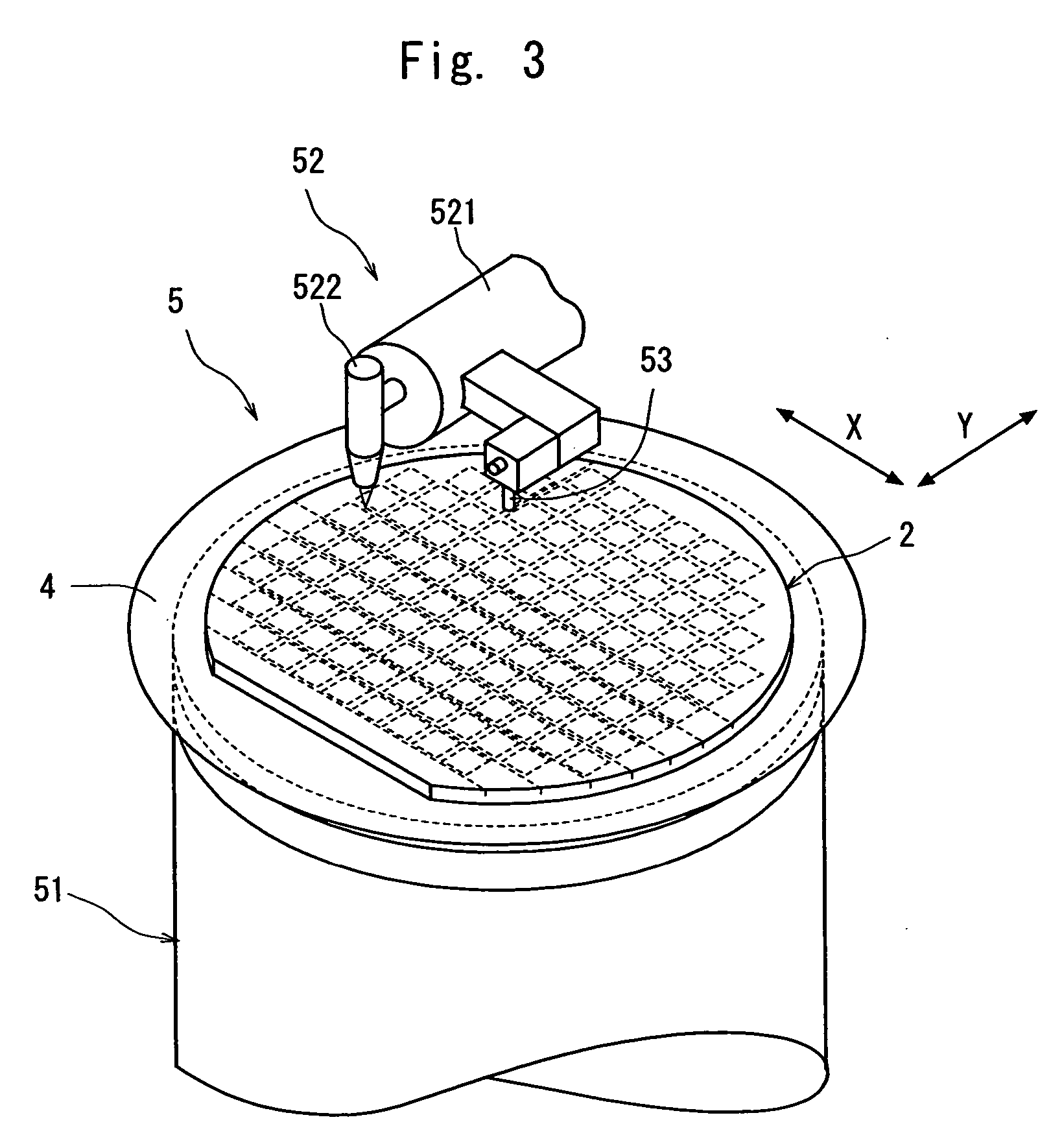
[0023] The front surface 2a side of the semiconductor wafer 2 constituted as described above is put on a support tape 4 which is composed of a synthetic resin sheet such as a polyolefin sheet ...


PUM

PropertyMeasurementUnit
wavelengthaaaaaaaaaa
repetition frequencyaaaaaaaaaa

Abstract

A method of dividing a wafer having a plurality of devices, which are formed in a plurality of areas sectioned by streets formed in a lattice pattern on the front surface and test metal patterns which are formed on the streets, comprising: a metal pattern breaking step for forming a break line in the test metal patterns by applying a pulse laser beam having permeability to the wafer to the rear surface of the wafer with its focal point set to a position near the test metal patterns; a deteriorated layer forming step for forming a deteriorated layer along the streets above the break lines in the inside of the wafer by applying a pulse laser beam having permeability to the wafer to the rear surface of the wafer with its focal point set to a position above the break lines in the inside of the wafer; and a dividing step for dividing the wafer into individual chips along the deteriorated layers of the wafer by exerting external force to the wafer having the deteriorated layers formed therein.

Description

FIELD OF THE INVENTION [0001] The present invention relates to a method of dividing a wafer having a plurality of devices, which are formed in a plurality of areas sectioned by streets formed in a lattice pattern on the front surface thereof, and having test metal patterns which are formed on the streets along the streets. DESCRIPTION OF THE PRIOR ART [0002] As known to people of ordinary skill in the art, in the production process of a semiconductor device, individual semiconductor chips are manufactured by cutting a semiconductor wafer comprising devices such as IC's or LSI's which are formed in a plurality of areas sectioned by break lines called “streets” arranged in a lattice pattern on the front surface of a substantially disk-like semiconductor substrate, along the streets to divide it into the areas each having a device formed thereon. [0003] Most of the above semiconductor wafers have a plurality of test metal patterns called “test element group (TEG)” for testing the funct...

Claims


Application Information

Patent Timeline
Patent Type & Authority Applications(United States)
IPC IPC(8): H01L21/78B23K26/00B23K26/364B23K26/38
CPCB23K26/4075H01L21/78B28D5/0011B23K26/40B23K2103/50
Inventor NAKAMURA, MASARUNAGAI, YUSUKE
Owner DISCO CORP
Why Eureka
Try Eureka