Methods of selectively forming an epitaxial semiconductor layer using ultra high vacuum chemical vapor deposition technique and batch-type ultra high vacuum chemical vapor deposition apparatus used therein

a technology of chemical vapor deposition and selective etching, which is applied in the direction of crystal growth process, polycrystalline material growth, chemically reactive gas growth, etc., can solve the problem of difficult suppression of the short channel effect of the mos transistor, the epitaxial growth rate and selective etching rate may be non-uniform, and the epitaxial growth rate and selective etching rate may be low

Inactive Publication Date: 2007-01-11
SAMSUNG ELECTRONICS CO LTD
View PDF13 Cites 29 Cited by
  • Summary
  • Abstract
  • Description
  • Claims
  • Application Information

AI Technical Summary

Problems solved by technology

Therefore, when the LPCVD SEG process is used in the fabrication of highly integrated semiconductor devices, it may be difficult to suppress a short channel effect of the MOS transistors.
As a result, an epitaxial growth rate and a selective etching rate may be non-uniform throughout the semiconductor substrates loaded in a reaction furnace or throughout the surface of each of the semiconductor substrates.
However, the single wafer type UHVCVD epitaxial growth process is performed at a low process temperature, thereby exhibiting low epitaxial growth rates.
Hence, the single wafer type UHVCVD epitaxial growth process may have a disadvantage of low throughput.

Method used


Image

  • Methods of selectively forming an epitaxial semiconductor layer using ultra high vacuum chemical vapor deposition technique and batch-type ultra high vacuum chemical vapor deposition apparatus used therein
  • Methods of selectively forming an epitaxial semiconductor layer using ultra high vacuum chemical vapor deposition technique and batch-type ultra high vacuum chemical vapor deposition apparatus used therein
  • Methods of selectively forming an epitaxial semiconductor layer using ultra high vacuum chemical vapor deposition technique and batch-type ultra high vacuum chemical vapor deposition apparatus used therein

Examples


examples

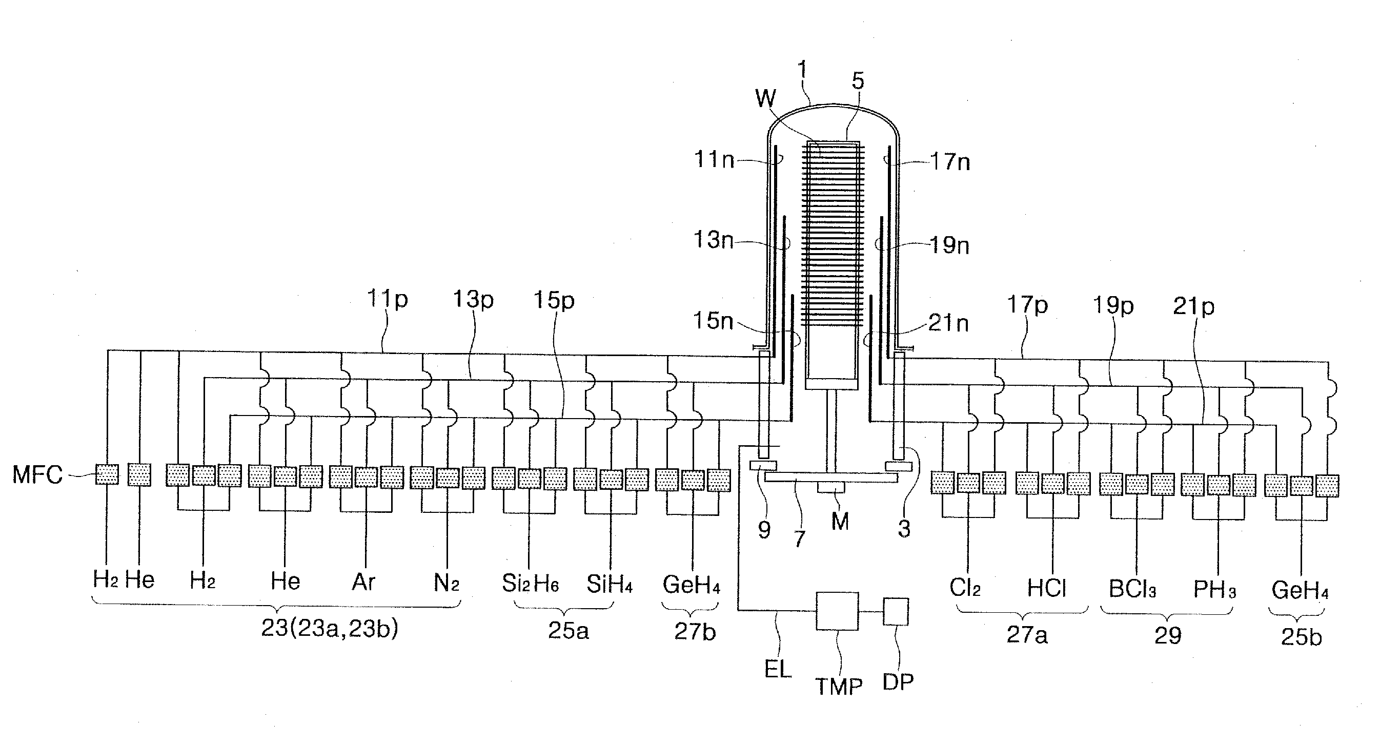
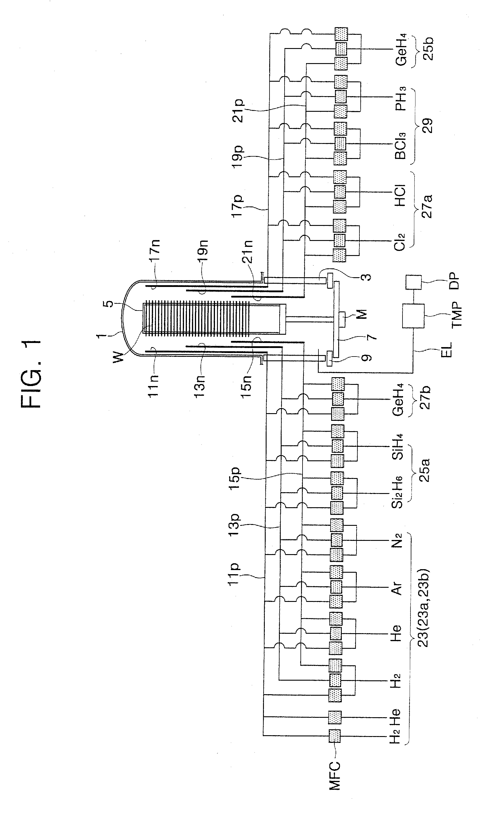
[0067]FIG. 5 is a graph showing the relationship between the etch uniformity and the carrier gas of SEG processes in accordance with embodiments of the present invention. In FIG. 5, the abscissa represents split conditions of the carrier gas, the left ordinate represents first etch uniformity UE1 corresponding to wafer etch uniformity, and the right ordinate represents second etch uniformity UE2 corresponding to etch uniformity within the wafer. After repeatedly applying only the selective etching process (step 45 of FIG. 2A) to semiconductor wafers having polysilicon layers for a certain period, the etch uniformities UE1 and UE2 were calculated from variations in the thickness of the polysilicon layers. The selective etching process was performed using main process conditions described in the following table [Table 1]. In the present experiment, a selective etching gas was injected through three gas nozzles as described with reference to FIG. 1.

TABLE 1Process parametersProcess co...


PUM

PropertyMeasurementUnit
temperatureaaaaaaaaaa
pressureaaaaaaaaaa
pressureaaaaaaaaaa

Abstract

Provided are methods of selectively forming an epitaxial semiconductor layer using an ultra high vacuum chemical vapor deposition (UHVCVD) technique. One embodiment is directed to a method that includes loading a substrate having an insulating layer pattern into a reaction furnace. The reaction furnace is evacuated, and the substrate in the reaction furnace is heated to a temperature of about 550 to about 700° C. A semiconductor source gas is injected into the reaction furnace for a first duration to selectively form an epitaxial semiconductor layer on a region of the heated substrate. The semiconductor source gas remaining in the reaction furnace is then purged for a second duration. A selective etching gas is injected into the reaction furnace for a third duration to selectively remove semiconductor atoms adsorbed on surfaces of the insulating layer pattern. The selective etching gas remaining in the reaction furnace is then purged for a fourth duration. A carrier gas may be injected into the reaction furnace during at least the second to fourth durations.

Description

CROSS-REFERENCE TO RELATED APPLICATION [0001] This U.S. non-provisional patent application claims priority under 35 U.S.C. §119 from Korean Patent Application 2005-0061920 filed on Jul. 8, 2005, the entire contents of which are hereby incorporated by reference. BACKGROUND [0002] 1. Field of the Invention [0003] The present invention relates to selective epitaxial growth (SEG) processes employed in the fabrication of a semiconductor device and chemical vapor deposition (CVD) apparatus used therein and, more particularly, to methods of selectively forming an epitaxial semiconductor layer using a ultra high vacuum chemical vapor deposition (UHVCVD) technique and a batch-type ultra high vacuum chemical vapor deposition (UHVCVD) apparatus used therein. [0004] 2. Description of Related Art [0005] Semiconductor devices are manufactured using various unit processes. Among these unit processes, a selective epitaxial growth (SEG) process has been widely used in the fabrication of highly integ...

Claims


Application Information

Patent Timeline
Patent Type & Authority Applications(United States)
IPC IPC(8): C30B23/00C30B25/00C30B28/12C30B28/14
CPCC23C16/4408C30B29/06C30B25/02C23C16/45523C23C16/04H01L21/205
Inventor LEE, DEOK-HYUNGKANG, MIN-GUSHIN, YU-GYUNLEE, JONG-WOOK
Owner SAMSUNG ELECTRONICS CO LTD
Why Eureka
Try Eureka