Solid-state imaging device and method for manufacturing the same

a technology of solid-state imaging and manufacturing methods, which is applied in the field a manufacturing method, can solve the problems of the degradation of sensitivity and s/n ratio the increase in the size of solid-state imaging devices, and the difficulty of downsizing a product that comes with such a solid-state imaging device, etc., to achieve the effect of suppressing the degradation of sensitivity and s/n ratio

Inactive Publication Date: 2007-01-11
PANASONIC CORP
View PDF8 Cites 9 Cited by
  • Summary
  • Abstract
  • Description
  • Claims
  • Application Information

AI Technical Summary

Benefits of technology

[0018] Therefore, with the foregoing in mind, it is an object of the present invention to provide a solid-state imaging de...

Problems solved by technology

If the increase in the number of pixels results in an increase in the size of the solid-state imaging device, it becomes difficult to downsize a product that comes with such a solid-state imaging devi...

Method used


Image

  • Solid-state imaging device and method for manufacturing the same
  • Solid-state imaging device and method for manufacturing the same
  • Solid-state imaging device and method for manufacturing the same

Examples


embodiments

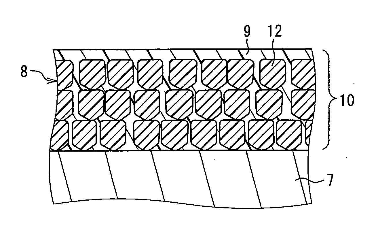
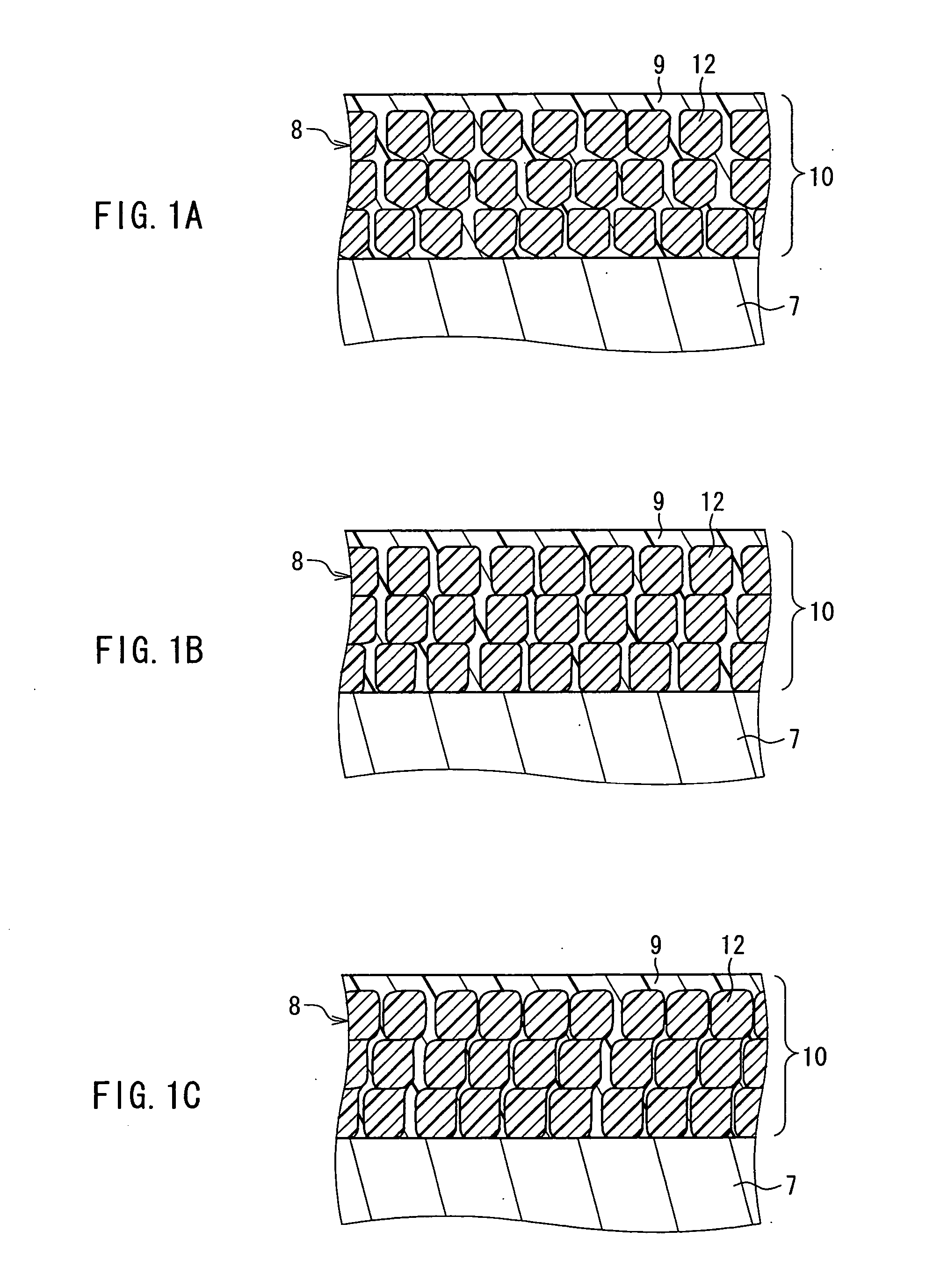
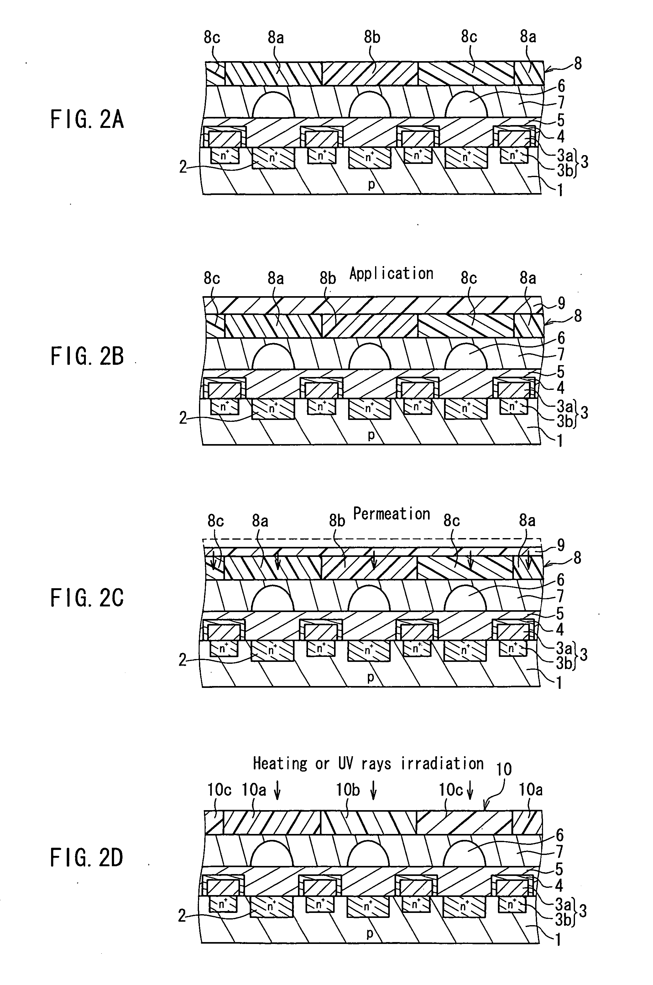
[0037] The following describes a solid-state imaging device and a method for manufacturing a solid-state imaging device according to embodiments of the present invention, with reference to FIG. 1 and FIG. 2. Firstly, the configuration of the solid-state imaging device of the present embodiment will be described below, with reference to FIG. 1. FIG. 1 is a partial cross-sectional view showing partially the configuration of the solid-state imaging device of one embodiment in the present invention, where FIGS. 1A to C show examples where the deposition states of colored particles are different from each other. FIGS. 1A to C illustrate only the lines appearing in their cross section.

[0038] As shown in FIGS. 1A to C, also in the present embodiment, a color filter 10 is formed at an upper layer of photodiodes serving as light-receptive elements in a similar manner to the conventional examples shown in FIG. 5 and FIG. 6 in the above section concerning the related art (see FIG. 2). The col...


PUM


Abstract

A solid-state imaging device includes: a plurality of light-receptive elements arranged in a matrix in a semiconductor substrate; and a plurality of color filters corresponding to the plurality of light-receptive elements, respectively. The color filters include a colored film formed by depositing colored particles at an upper layer of the plurality of light-receptive elements, and a resin with which gaps between the colored particles are filled. The resin with which the gaps between the colored particles are filled may be transparent or be colored.

Description

BACKGROUND OF THE INVENTION [0001] 1. Field of the Invention [0002] The present invention relates to a solid-state imaging device and a method for manufacturing the same. [0003] 2. Description of Related Art [0004] In recent years, solid-state imaging devices have been used for imaging devices of a digital still camera and a digital video camera and for image reading devices of a facsimile, a scanner and a copying machine, and the demands therefor have expanded. As major solid-state imaging devices, MOS-type solid-state imaging devices and CCD (charge-coupled device) type solid-state imaging devices are known. Recently, these solid-state imaging devices often are provided with color filters in order to capture a color image. [0005]FIG. 5 is a partial cross-sectional view showing the configuration of a conventional solid-state imaging device. The solid-state imaging device of FIG. 5 is a CCD type solid-state imaging device. As shown in FIG. 5, the solid-state imaging device includes ...

Claims


Application Information

Patent Timeline
IPC IPC(8): G01J3/50
CPCH01L27/14621H01L27/14623H04N9/045H01L27/14685H01L27/14868H01L27/14645H04N25/136H04N25/134
Inventor TAKEUCHI, YASUO
Owner PANASONIC CORP
Why Eureka
Try Eureka