
Apparatus and method for reducing drain modulation of high power transistor

Inactive Publication Date: 2007-01-11
SAMSUNG ELECTRONICS CO LTD
View PDF5 Cites 1 Cited by
  • Summary
  • Abstract
  • Description
  • Claims
  • Application Information

AI Technical Summary

Benefits of technology

[0010] Another object of exemplary embodiments of the present invention is to provide an apparatus for minimizing drain modulation and improving amplification characteristic of a transistor by using an adder and a bias unit.

Problems solved by technology

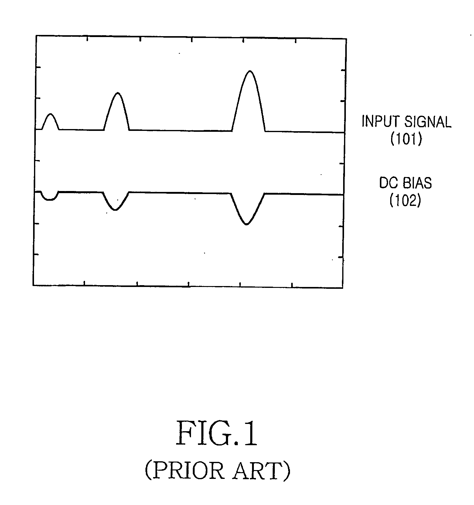
In the drain modulation, the AC component characteristic acts as power noise in the transistor of the high power amplifier, degrading performance of the transistor.
Hence, when the amplifier is implemented with actual transistors, the technical application of pre-distortion is difficult.
However, the drain modulation cannot be completely removed only using the capacitors.
Also, the use of the capacitors influences the switching speed of the transistor, resulting in the performance degradation of the transistor.
Moreover, the amplifier has to be designed to be large in size, thus increasing its price.
Consequently, the amplifier having the above-described structure has no benefit of performance in a real channel environment.

Method used


Image

  • Apparatus and method for reducing drain modulation of high power transistor
  • Apparatus and method for reducing drain modulation of high power transistor
  • Apparatus and method for reducing drain modulation of high power transistor

Examples


Embodiment Construction

[0018] The matters defined in the description such as a detailed construction and elements are provided to assist in a comprehensive understanding of the embodiments of the invention. Accordingly, those of ordinary skill in the art will recognize that various changes and modifications of the embodiments described herein can be made without departing from the scope and spirit of the invention. Also, descriptions of well-known functions and constructions are omitted for clarity and conciseness.

[0019] Hereinafter, an apparatus for reducing drain modulation of a high power transistor according to an exemplary embodiment of the present invention will be described in detail.

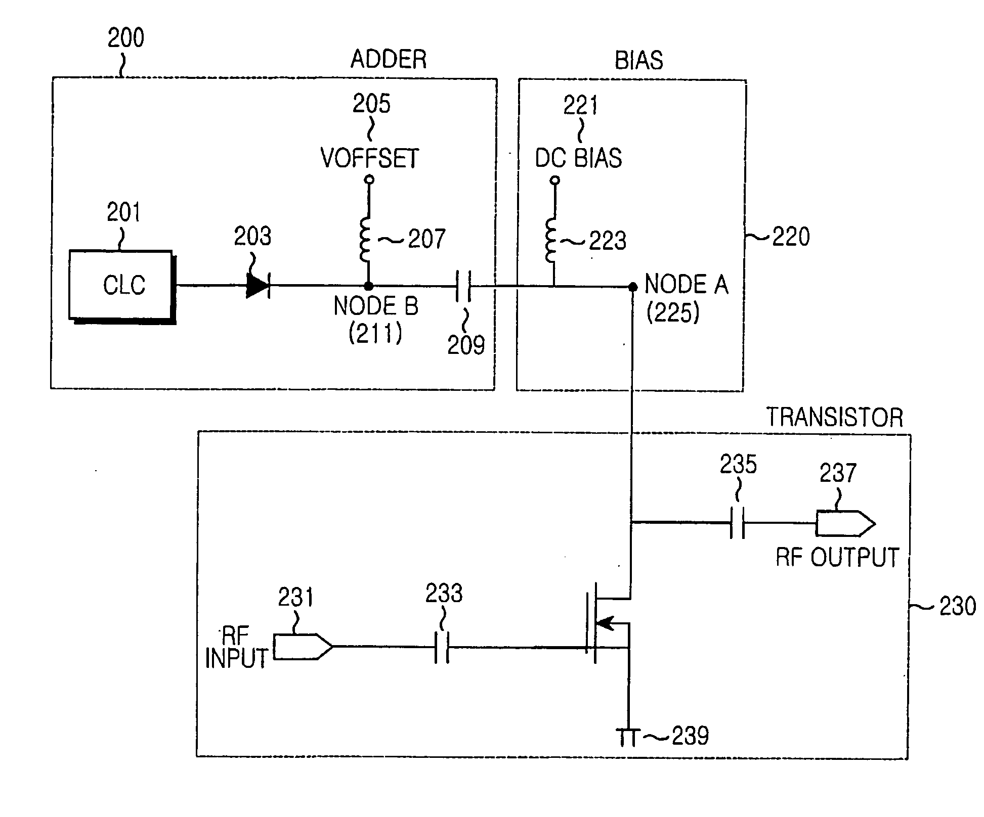
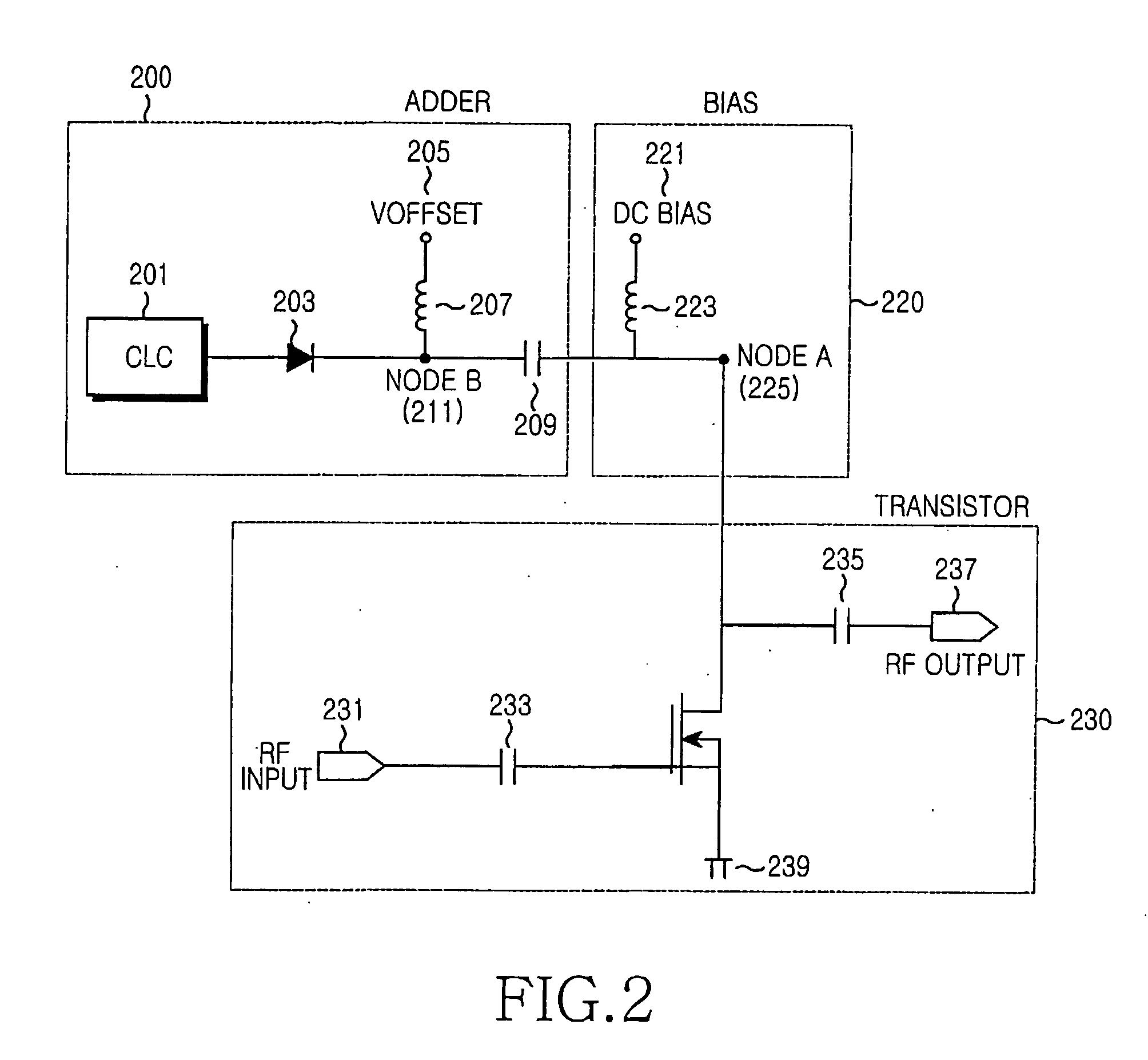
[0020]FIG. 2 is a circuit diagram of a high power amplifier with a reduced drain modulation according to an exemplary embodiment of the present invention.

[0021] Referring to FIG. 2, the high power amplifier includes an adder 200, bias unit 220, and transistor 230. The adder 200 supplies the bias unit 220 with a curr...


PUM


Abstract

An apparatus and a method for reducing drain modulation in a high power amplifier are provided, in which an adder supplies a current corresponding to a voltage reduced by a drain modulation, and a bias unit adds the current supplied from the adder to a DC bias and supplies the added current to a drain of a transistor. Accordingly, the drain modulation occurring in the transistor can be minimized and an output characteristic of the high power transistor can be improved.

Description

CROSS-REFERENCE TO RELATED PATENT APPLICATIONS [0001] This application claims the benefit under 35 U.S.C. § 119(a) of a Korean Patent Application filed in the Korean Intellectual Property Office on Jul. 7, 2005 and assigned Serial No. 2005-60999, the entire disclosure of which is hereby incorporated by reference. BACKGROUND OF THE INVENTION [0002] 1. Field of the Invention [0003] The present invention relates generally to a high power transistor. More particularly, the present invention relates to an apparatus and a method for reducing drain modulation of a high power transistor. [0004] 2. Description of the Related Art [0005] High power transistors (for example, Lateral Double diffused MOS (LDMOS), gallium arsenide (GaAs) transistor, and the like) for high power amplifiers have high power and use a current of several amperes. Specifically, in the case of a Code Division Multiple Access (CDMA) that amplifies a modulated signal, magnitude of the input signal continuously varies with ...

Claims


Application Information

Patent Timeline
IPC IPC(8): H03F3/04
CPCH03F1/301H03F3/193H03F1/3205H03F1/30H03F1/02
Inventor KIM, KYOUNG-TAE
Owner SAMSUNG ELECTRONICS CO LTD
Learn More