Semiconductor device

a technology of semiconductors and devices, applied in the field of semiconductor devices, can solve the problems of low production yield, high production cost, short retention time of cells, etc., and achieve the effect of improving refresh characteristics and suppressing the decrease of voltage levels

Inactive Publication Date: 2007-01-11
LONGITUDE LICENSING LTD
View PDF9 Cites 72 Cited by
  • Summary
  • Abstract
  • Description
  • Claims
  • Application Information

AI Technical Summary

Benefits of technology

[0021] In a semiconductor device to which double refresh is applicable, a voltage level of a power supply voltage VPP generated by a VPP power supply circuit inside a chip is monitored and an optimum double refresh operation mode is determined with reference to the voltage level. Thus, it is possible to suppress a decrease in voltage level of the power supply voltage VPP and to improve refresh characteristics in the double refresh.

Problems solved by technology

However, due to the limitation in number of redundant circuits (that is, the redundant memory cells), some of the memory cells having short retention times may be kept present without being relieved.
This results in a low production yield and a high production cost.
However, in case where a large number of redundant circuits are provided, the semiconductor device is inevitably increased in chip area.
After all, the production cost is increased.
This results in an increase in chip cost.
As described above, the semiconductor device has a problem that, because of presence of the memory cells having short retention times, the yield is decreased.
This results in an increase in chip cost.

Method used


Image

  • Semiconductor device
  • Semiconductor device
  • Semiconductor device

Examples


first embodiment

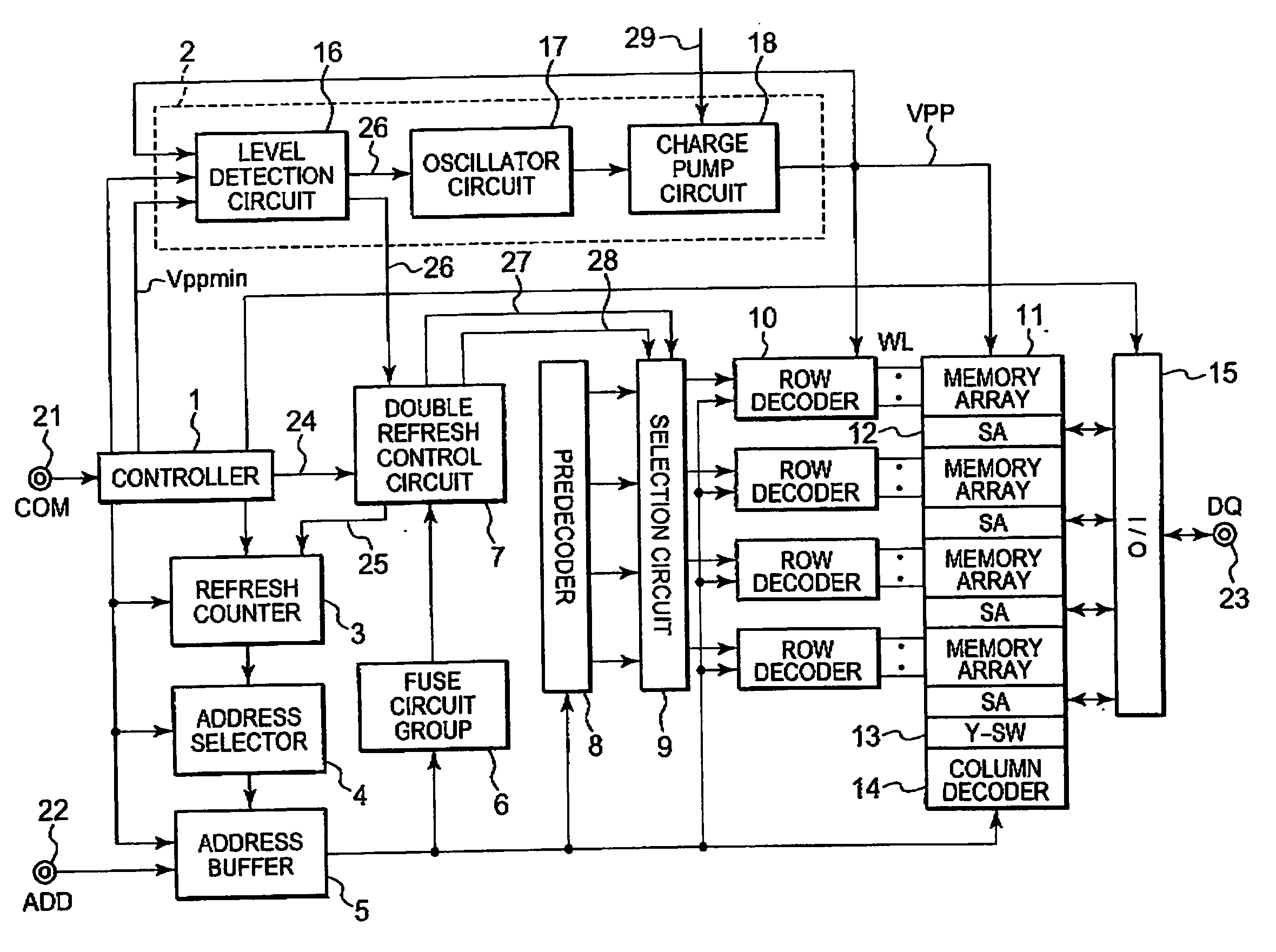
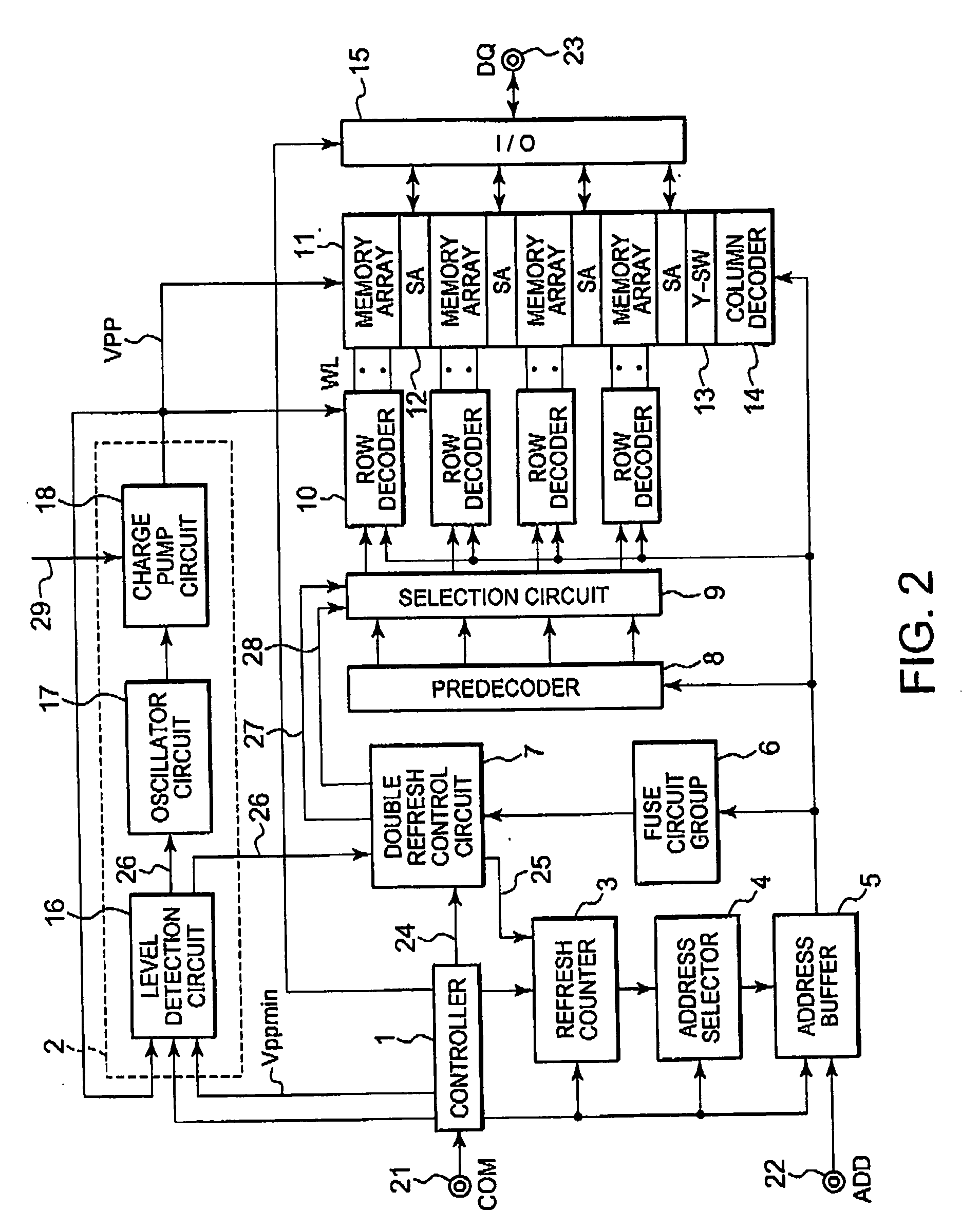
[0028] Referring to FIGS. 2 and 3, a first embodiment of this invention will be described. In this embodiment, time-division refresh or serial refresh is selectively carried out as a double refresh operation mode. In case where a power supply voltage VPP generated by a VPP power supply circuit is not lower than a predetermined voltage, time-division refresh is carried out. In the time-division refresh, one refresh cycle is time-divided and refresh operations are carried out for a particular word line and a pair word line in the one refresh cycle. In case where the power supply voltage VPP is lower than the predetermined voltage, serial refresh is performed in which a refresh operation for a particular word line is performed in one refresh command cycle and a refresh operation for a pair word line is inserted in a next refresh command cycle.

[0029] At first referring to FIG. 2, a semiconductor device according to this invention will be described. In FIG. 2, a part of a structure of t...

second embodiment

[0065] Referring to FIGS. 2 and 4, a second embodiment of this invention will be described. In this embodiment, when the power supply voltage VPP is higher and lower than the lower limit voltage Vppmin, parallel refresh and serial refresh are selected as the double refresh operation mode, respectively.

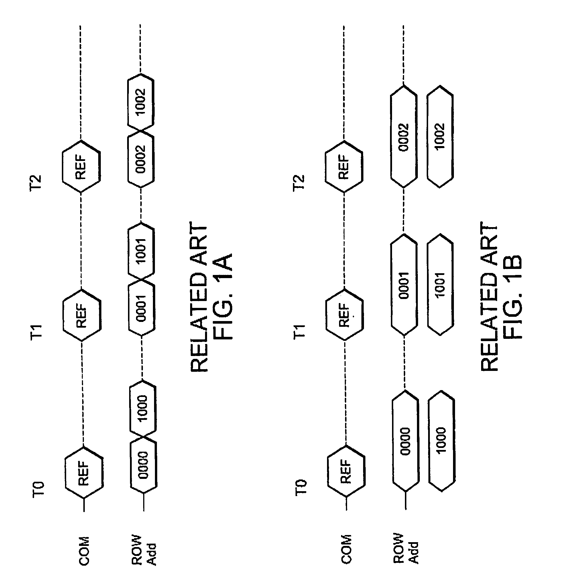
[0066]FIG. 4 shows the refresh commands REF as the commands (COM), the row addresses (ROW Add) selected upon input of the refresh commands REF, and the power supply voltage VPP. At the time instant T0, the first refresh command REF is supplied and the word line “0000” is refreshed. The pair word line “1000” is to be subjected to the double refresh and the double refresh is performed. At the time instant T0, the power supply voltage VPP is higher than the lower limit voltage Vppmin of the design value. Therefore, in one refresh cycle, the word line “0000” and the pair word line “1000” are simultaneously refreshed.

[0067] Thus, refreshing the word line and the pair word line simultaneou...


PUM


Abstract

In a semiconductor device, an internally-generated power supply voltage VPP is monitored. If the internally-generated power supply voltage VPP is lower than a lower limit voltage, serial refresh is selected as a double refresh operation mode. In the serial refresh, double refresh for a pair address is inserted in a next refresh cycle. By the serial refresh, decrease of the internally-generated power supply voltage VPP is suppressed.

Description

[0001] This application claims priority to prior Japanese patent application JP 2005-160948, the disclosure of which is incorporated herein by reference. BACKGROUND OF THE INVENTION [0002] This invention relates to a semiconductor device and, in particular, to a semiconductor device in which a double refresh operation mode is changed with reference to an internally-generated power supply voltage VPP (hereinafter will simply be referred to as a power supply voltage VPP) a power supply voltage level upon refreshing and relieving a memory cell. [0003] As a semiconductor device, a dynamic random access memory (hereinafter referred to as “DRAM”) having a large capacity and randomly accessible is known. The DRAM holds memory information as electric charges stored in capacitors of memory cells. It is therefore required to perform a refresh operation by reading the memory information before the electric charges fade away, amplifying the memory information, and restoring the memory informati...

Claims


Application Information

Patent Timeline
Patent Type & Authority Applications(United States)
IPC IPC(8): G11C7/00
CPCG11C5/063G11C5/147G11C2211/4068G11C11/406G11C11/4074G11C8/08
Inventor DONO, CHIAKIKOSHIKAWA, YASUJI
Owner LONGITUDE LICENSING LTD
Why Eureka
Try Eureka