
Optical Surface Inspection

a surface and optical technology, applied in the direction of instruments, material analysis, measurement devices, etc., can solve the problems of not meeting the stringent requirements, time-consuming and error-prone, and cumbersome successive displacement of the semi-conductor wafer for the acquisition of single images,

Inactive Publication Date: 2007-01-11
IBM CORP
View PDF16 Cites 21 Cited by
  • Summary
  • Abstract
  • Description
  • Claims
  • Application Information

AI Technical Summary

Benefits of technology

[0013] According to a further preferred embodiment of the invention, the at least first and second images are acquired simultaneously or in partially overlapping time intervals. This allows for a remarkable decrease of optical inspection time by simultaneously maintaining a required resolution. Simultaneous acquisition of the at least first and the at least second images may also be realized by superimposing respective first and second optical fields before the image acquisition takes place. In this way the superposition step can be implemented all optically by superimposing of the at least first and second optical fields providing first and second images of respective surface segments.
[0038] According to a further preferred embodiment of the invention, the imaging means further comprise an array of at least first and second microlenses. Preferably, the array of microlenses is adapted to the diffractive optical element. For example, the diffractive optical element splits a light beam into an array of 5×5 spatially separated light beams. This array of light beams then passes through the configurable SLM and enters an appropriate array of microlenses. In this configuration, the array of microlenses provides sufficient imaging of each of the 25 separate light beams. Preferably, the optical inspection apparatus is provided with a whole set of microlens arrays and diffractive optical elements that allows to universally adapt the optical inspection apparatus to various geometries of periodic structures on various types of substrates that become subject to surface inspection.

Problems solved by technology

Obviously, this is rather cumbersome, time intensive as well as error prone.
However, acquisition as well as comparison of various images of periodic structures typically requires sequential acquisition of single images.
Even though surface inspection may reach a high degree of automation, a successive displacement of the semi-conductor wafer for acquisition of single images is still rather time intensive and may still not fulfill the stringent requirements of inspection throughput within a mass production process.
However, an enlarging of a field of view, hence increasing of an inspection area, of an optical inspection system can only be realized at the expense of resolution decrease.
An increase of the field of view therefore inevitably comes along with a decrease in resolution that might no longer guarantee a sufficient quality control.
However, laser scanning usually does not provide an optical image of the inspected structures nor does it allow sophisticated defect classification.

Method used


Image

  • Optical Surface Inspection
  • Optical Surface Inspection
  • Optical Surface Inspection

Examples


Embodiment Construction

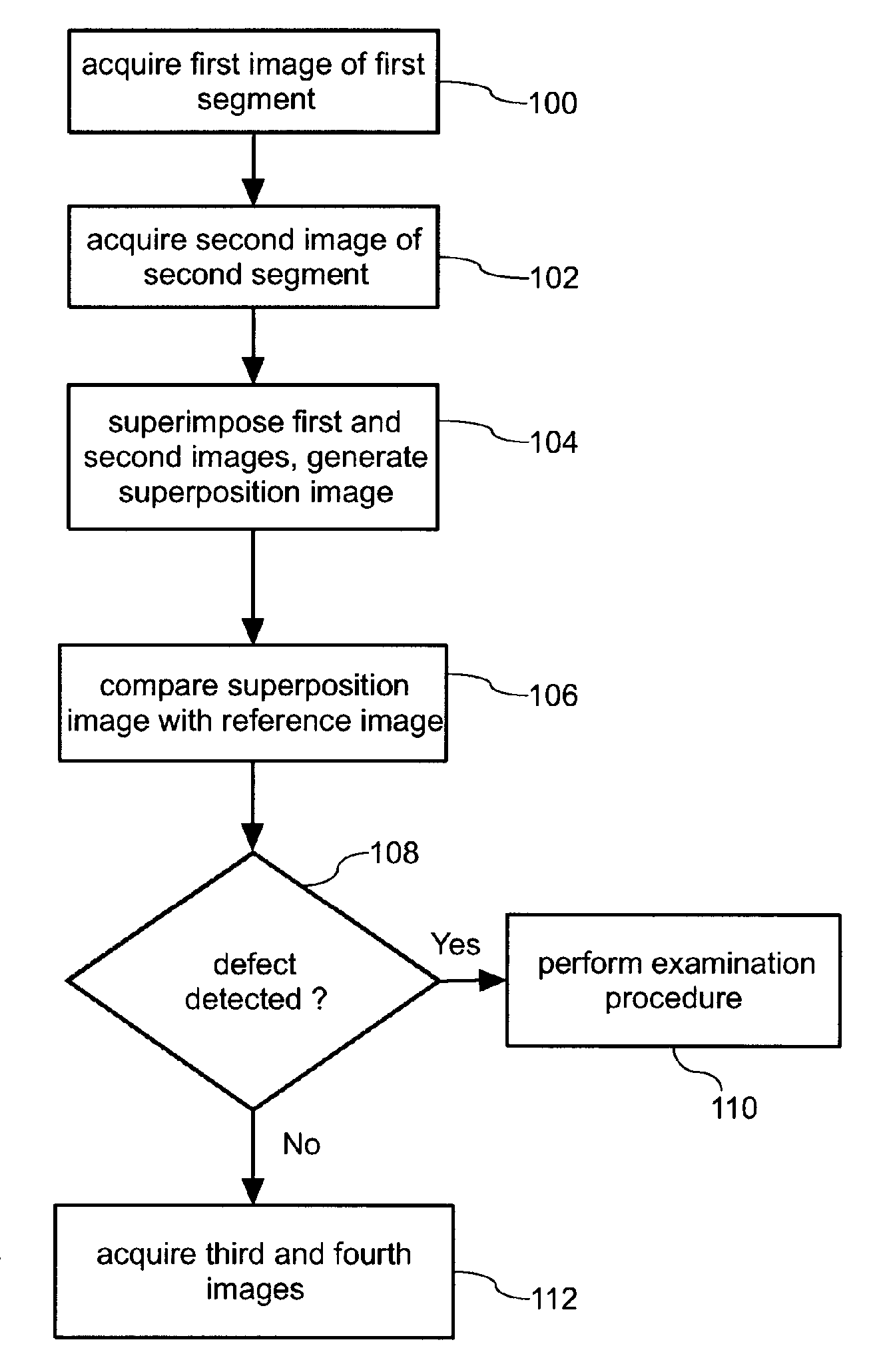
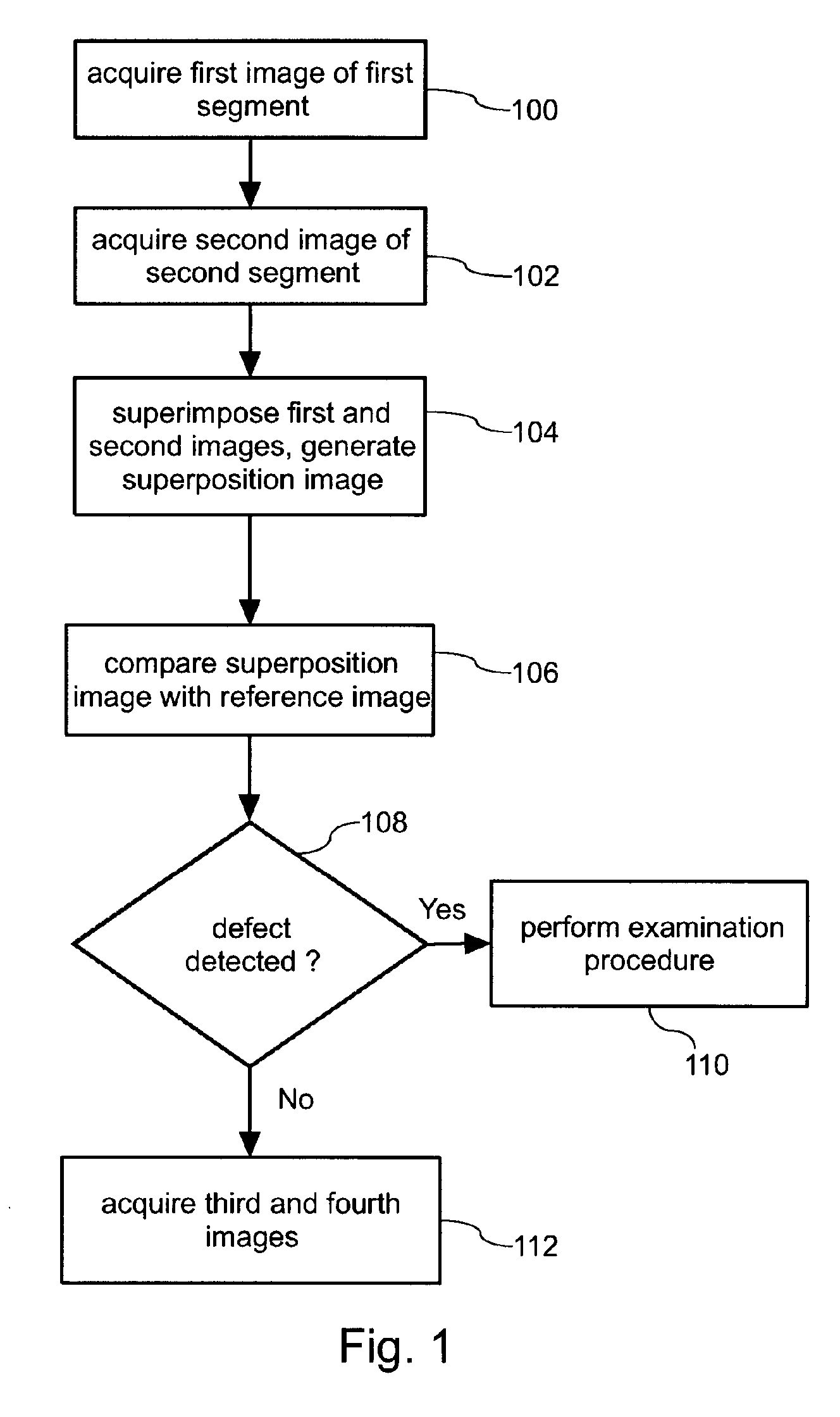
[0049]FIG. 1 illustrates a flow chart for acquiring at least a first and a second image of respective first and second segments of the surface, to superimpose the first and second images for generating a superposition image and to compare the superposition image with a reference image in order to detect a surface defect. Therefore in a first step 100, a first image of the first segment is acquired. Thereafter in step 102, a second image of a second segment is acquired correspondingly. According to the invention, at least first and second images have to be acquired. Acquisition of images as well as superposition of images is by no means restricted to only two images. Moreover, the number of acquired and superimposed images may be adapted to required specifications of the surface inspection system.

[0050] In step 104 the acquired images are superimposed and a superposition image is generated thereof. Acquisition of images and their superposition are illustrated as sequential steps 100...


PUM


Abstract

The present invention provides a method, an optical inspection apparatus as well as a computer program product for optical inspection of a surface. The optical inspection apparatus can be effectively applied for optical inspection of periodic structures on e.g. a semi-conductor wafer for the purpose of quality control. By effectively splitting a light beam into a plurality of spatially separated light beams and by selective usage of these light beams, various surface segments of the surface can be inspected simultaneously by superposition of respective images. A resulting superposition image can then be compared with a reference image for detection of defects of the surface.

Description

TECHNICAL FIELD [0001] The present invention relates to the field of optical inspection of a surface for detecting defects of the surface. DESCRIPTION OF THE PRIOR ART [0002] The control of quality is an important step in the manufacturing process of structured substrates, as e.g. semi-conductor wafers. Typically, semi-conductor wafers provide a grid or an array of periodic structures, each of which representing an integrated circuit or a chip. Since nowadays, semi-conductor wafers are predominantly subject to mass production, a subsequent quality control has to provide a throughput or inspection capacity that corresponds to the mass production process. For quality control of surfaces, like structured substrates, optical inspection techniques are a predestinated means. In principle, optical inspection techniques provide a fast, reliable and intuitive approach to the detection of surface defects of e.g. a structured substrate. [0003] Generally, optical surface inspection can be perfo...

Claims


Application Information

Patent Timeline
Patent Type & Authority Applications(United States)
IPC IPC(8): G06K9/00
CPCG01N21/95607H01L21/67288G01N2201/0675
Inventor BRASEN, GERNOTLAUE, CHRISTIANLOEFFLER, MATTHIASTHEUER, HEIKO
Owner IBM CORP
Learn More