Method of manufacturing a CMOS image sensor

a manufacturing method and image sensor technology, applied in the direction of diodes, semiconductor devices, electrical apparatuses, etc., can solve the problems of low resolution of image sensors and cross talk nois

Inactive Publication Date: 2007-01-11
UNITED MICROELECTRONICS CORP
View PDF7 Cites 28 Cited by
  • Summary
  • Abstract
  • Description
  • Claims
  • Application Information

AI Technical Summary

Problems solved by technology

As we know the prior CMOS image sensor has low resolution and cross talk noise.
The important issue of the subject is how to i

Method used


Image

  • Method of manufacturing a CMOS image sensor
  • Method of manufacturing a CMOS image sensor
  • Method of manufacturing a CMOS image sensor

Examples


Embodiment Construction

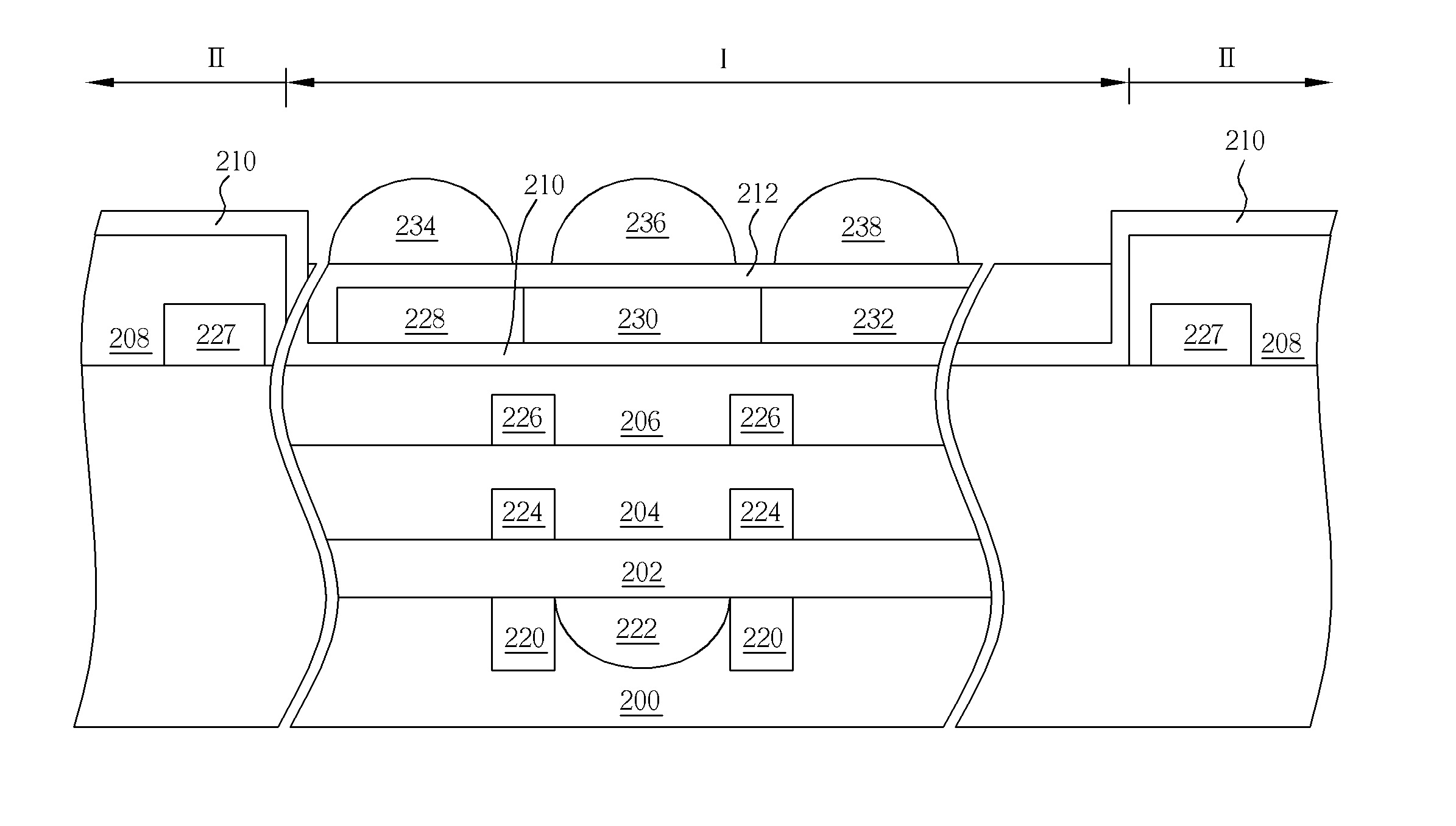
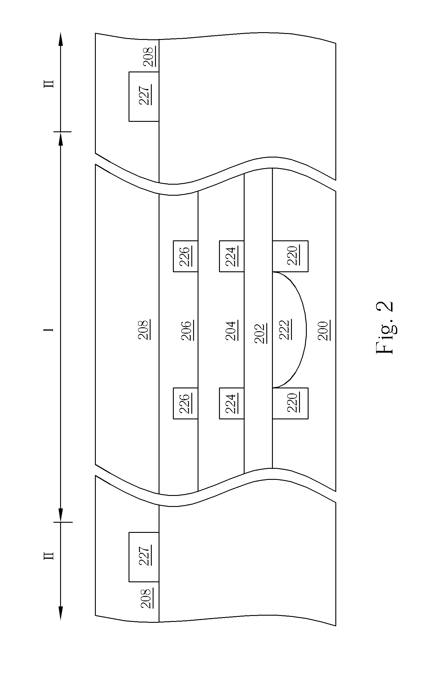
[0015] Please refer to FIG. 2 to 7, FIG. 2 to 7 are the schematic diagram of manufacturing the CMOS image sensor forms on the semiconductor substrate according to the present invention. As FIG. 2 shows, the semiconductor substrate 200 divides into the pixel array area I and the logic area II. In the pixel array area I, the semiconductor substrate 200 comprises the plurality of shallow trench isolations 220 and the plurality of photodiodes 222. Each of the photodiode 222 contacts electrically with the correspondingly CMOS (not shown). The shallow trench isolation 220 uses as the insulator of the photodiode 222 and the adjacent photodiode 222, that prevents the short circuit from the photodiode 222 contacts the other components.

[0016] In the present invention, the flat layer 202 is formed on the semiconductor substrate 200 to cover the photodiode 222 and CMOS (not shown), the plurality of metal layers 224 and the dielectric layer 204 are formed on the flat layer 202, then, the plural...


PUM


Abstract

The present invention relates to the method of manufacturing an image sensor, the method comprising providing a semiconductor substrate, which comprises a pixel array area and a logic area, a plurality of the photodiodes are formed on the semiconductor substrate of the pixel array area, a multilevel interconnect process is processed on the semiconductor substrate, a passivation is doping on the pixel array area and the logic area, removing the passivation on the pixel array area, and a plurality of the color filter arrays are formed on the pixel array area and correspond to the photodiode individually.

Description

BACKGROUND OF THE INVENTION [0001] 1. Field of the Invention [0002] The present invention relates to a method of manufacturing an image sensor, more particularly to, a method of manufacturing a CMOS image sensor. [0003] 2. Description of the Prior Art [0004] The CMOS image sensor applies in digital electrical products recent years. For example, the line CMOS image sensor majors the scanner and the plane CMOS majors the digital camera. Because the standard CMOS manufacture and the recent semiconductor equipment and technology could manufacture the CMOS image sensor, the yield of the CMOS image sensor becomes greater. [0005] Please refer to FIG. 1, FIG. 1 is a schematic diagram of manufacturing the CMOS image sensor 140 forms on the semiconductor substrate 100 according to the prior art. The semiconductor substrate 100 comprises a plurality of shallow trench isolations 120 and a plurality of photodiodes 122 which electrically contacts at least a correspondingly CMOS (not shown). The s...

Claims


Application Information

Patent Timeline
IPC IPC(8): H01L31/113H01L31/062H01L21/00
CPCH01L27/14621H01L27/14627H01L27/14632H01L27/14689H01L27/14685H01L27/14687H01L27/14643
Inventor LI, SHENG-CHIN
Owner UNITED MICROELECTRONICS CORP
Why Eureka
Try Eureka