Bitmap cluster analysis of defects in integrated circuits

Active Publication Date: 2007-01-11
ONTO INNOVATION INC
View PDF6 Cites 0 Cited by
  • Summary
  • Abstract
  • Description
  • Claims
  • Application Information

AI Technical Summary

Benefits of technology

[0020] One embodiment of the bit clustering and aggregation system and method in accordance with the present invention provides many advantages over conventional bitmap analysis systems and techniques, which make the bit clustering and aggregation system and method in accordance with the present invention more useful to semiconductor manufacturers. The bit clustering and aggregation system and method in accordance with the various embodiments of the present invention identify random and systematic bitmap failed patterns. The system may be fully automated and is easy to use, so that no extra training is necessary to make use of the bit clustering and aggregation system. The system generates an output preferably in the form of a bit cluster analysis report that is easy to interpret and understand.
[0021] In accordance with one preferred embodiment of the present invention, clustering is provided such that when defining a bit cluster pattern, a user has the following options: 1) selecting a radius specified by a number of “good” bits away from another fail bit before the current fail bit can be classified as part of the original bit cluster; 2) selecting a minimum count of fail bits in a bit cluster; and 3) selecting a maximum count of fail bits in a bit cluster. One embodiment of the bit clustering and aggregation system and method in accordance with the present invention may receive a defect data set. When a defect data set is received, the bit clustering and aggregation system and method in accordance with the present invention starts with a fail bit and searches for neighboring fail bits. The bit clustering and aggregation system and method use the specified radius to qualify the found fail bits to be part of the cluster or not. If the minimum count of fail bits is not met, the bit clustering and aggregation system and method will stop searching and move to the next fail bit. If the minimum count of fail bits is met, the bit clustering and aggregation system and method will continue to search for the next fail bit until it reaches the maximum fail bit count specified by the user. Aggregation is provided such that once clusters have been classified, the number of clusters that have the exact match or partial match to each other is counted. The user has the option to preferably set the partial match as a threshold count to establish a match. The bit clustering and aggregation system and method in accordance with the present invention provide a defect bitmap analysis tool that is more powerful and flexible than conventional tools.

Problems solved by technology

The occurrence of defects may cause lower yield in the final semiconductor product, where yield may be defined as the number of functional devices produced by the process as compared to the theoretical number of devices that could be produced assuming no bad devices.
There are two major problems that arise with this technique.
Second, these seemingly random individual bits and groups of bits are sometimes systematic in nature, meaning that they almost always failed certain ways.

Method used


Image

  • Bitmap cluster analysis of defects in integrated circuits
  • Bitmap cluster analysis of defects in integrated circuits
  • Bitmap cluster analysis of defects in integrated circuits

Examples


Embodiment Construction

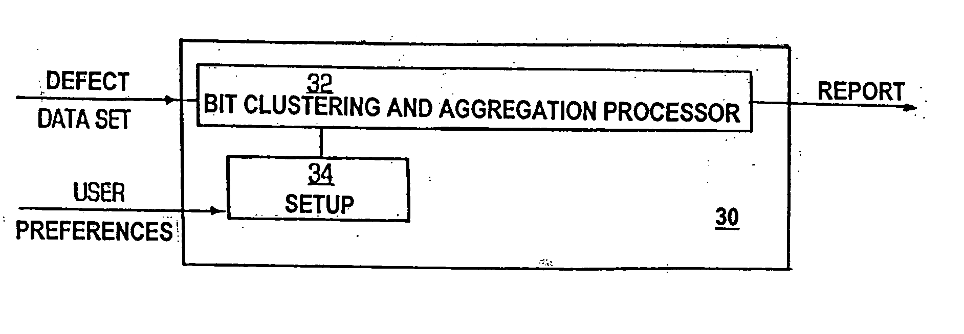
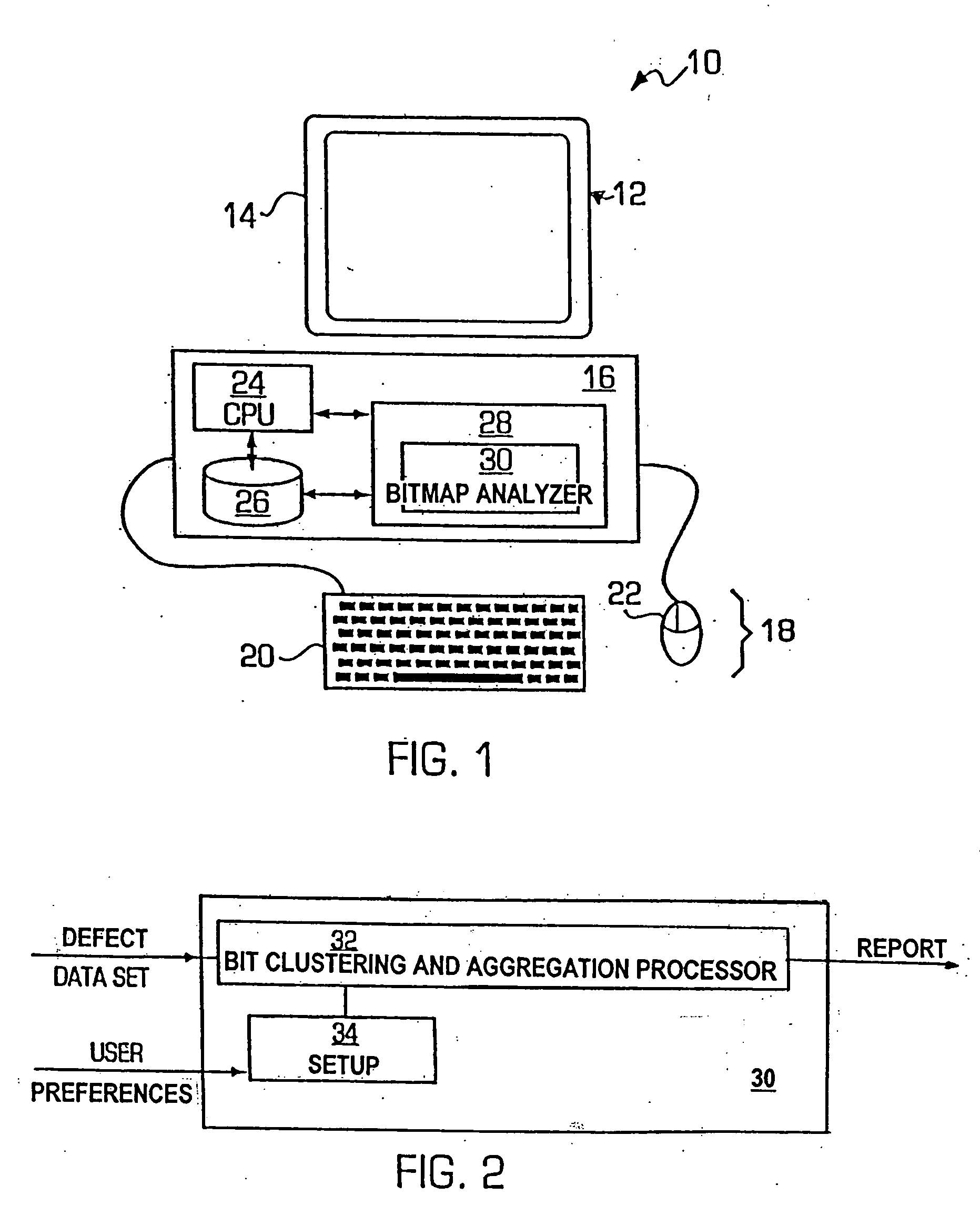
[0032] The present invention is particularly applicable to a computer-implemented software-based defect analysis system and method, and it is in this context that the various embodiments of the present invention will be described. It will be appreciated, however, that the defect analysis system and method in accordance with the present invention have greater utility, since they may be implemented in hardware or may incorporate other modules or functionality not described herein.

[0033]FIG. 1 is a block diagram illustrating an example of a defect analysis system 10 in accordance with one embodiment of the present invention implemented on a personal computer 12. In particular, the personal computer 12 may include a display unit 14, which may be a cathode ray tube (CRT), a liquid crystal display, or the like; a processing unit 16; and one or more input / output devices 18 that permit a user to interact with the software application being executed by the personal computer. In the illustra...


PUM


Abstract

A system and method for defect analysis are disclosed wherein a defect data set is input into the system. A radius value is selected by a user, which is the maximum number of bits that bit failures can be separated from one another to be considered a bit cluster. When a defect data set is received, the system and method start with a fail bit and search for neighboring fail bits. The specified radius is used to qualify the found fail bits to be part of the bit cluster or not. If a minimum count of fail bits is not met, the system and method will stop searching- and move to the next fail bit. If a minimum count of fail bits is met, the search continues for the next fail bit until the maximum fail bit count specified by the user is reached. Aggregation is provided such that once bit clusters have been classified, the number of clusters that have the exact match or partial match to each other is counted. The user may set the partial match as a threshold count to establish a match.

Description

BACKGROUND OF THE INVENTION [0001] 1. Field of the Invention [0002] The present invention relates generally to a system and method for quality control of integrated circuits manufactured by a semiconductor manufacturing process and, more particularly, to a system and method for analyzing defects in integrated circuits manufactured using a semiconductor fabrication process. [0003] 2. Description of the Prior Art [0004] The semiconductor manufacturing industry is continually evolving its fabrication processes and developing new processes to produce smaller and smaller geometries of the semiconductor devices being manufactured, because smaller devices typically generate less heat and operate at higher speeds than larger devices. Currently, a single integrated circuit chip may contain over one billion patterns. The occurrence of defects may cause lower yield in the final semiconductor product, where yield may be defined as the number of functional devices produced by the process as comp...

Claims


Application Information

Patent Timeline
IPC IPC(8): G11C29/00
CPCG01R31/318533G11C2029/5604G11C29/56008G11C29/56
Inventor HO, TOMBUCKHEIT, JONATHANWANG, WEIDONGSUN, XIN
Owner ONTO INNOVATION INC
Why Eureka
Try Eureka