Check patentability & draft patents in minutes with Patsnap Eureka AI!

Integrated scannable interface for testing memory

a scannable interface and memory technology, applied in the direction of measurement devices, error detection/correction, instruments, etc., can solve the problems of defect level, increase in the testing requirements for each chip, and defect level that goes beyond the control of process and design

Inactive Publication Date: 2007-01-11
STMICROELECTRONICS PVT LTD
View PDF11 Cites 7 Cited by
  • Summary
  • Abstract
  • Description
  • Claims
  • Application Information

AI Technical Summary

Benefits of technology

[0008] A need is therefore felt for a minimal area and high-speed integrated scan interface for testing memories that minimizes the timing faults of the testing system. In some embodiments. the present invention converts the latched interface into a flip-flop interface during test / scan mode. In some applications, the present invention is useful to measure the timing defects between the latches of the interface to thereby enhance the observation of the system for test and debugging. According to another aspect of the invention, high-speed patterns are captured at the input of the system so that speed binning is possible at the memory interface.
[0011] The present invention also provides a memory device having a plurality of storage cells for storing data, an address decoding device or decoder for receiving an address value and selecting cells from said plurality of storage cells corresponding to the address value, an input mechanism or device for storing data in the plurality of storage cells, an output mechanism or device that outputs data from the plurality of storage cells, a controller for enabling said address decoder, input device and output device, a high speed scan chain interface receiving enabling signals from the controller and coupled to the address decoder, input device and output device for providing high-speed and minimal area testing of the memory device.

Problems solved by technology

The increasing complexity on chip and of chip designs is inducing more defects in System on Chip (SoC) designs, and these defects are causing an increase in the testing requirements for each chip.
A robust design and a very well controlled process can reduce the defect level in the memory, but, unfortunately in the newer technologies, as the gate lengths shrink, the defect level goes beyond the control of process and of the design as well.
Typically, the interfaces which are being used to test the memory in the current methodologies add a lot on the input of the memory as well because they do not penetrate much inside the memory hierarchy to increase the observability.
As result, the conventional memory interface circuits are additional overheads to the memory.
Further, as these interfaces are not embedded inside the memory, it adds on to the cost of plugging it with the memory and increase the difficulty of measuring the timing defects between the system flip flops.
It is therefore very difficult to predict whether the fault is in the memory or is at the interface.
The testing techniques disclosed by the aforementioned patent do not take into account area constraints for a typical SOC design.
Further, the conventional interfaces, which are being used to test the memory in the current methodologies, add a lot on the input of the memory, and they do not penetrate much inside the memory hierarchy to increase the observability.
The memory interfaces, which have been proposed and are being used lack several desirable properties.

Method used


Image

  • Integrated scannable interface for testing memory
  • Integrated scannable interface for testing memory
  • Integrated scannable interface for testing memory

Examples


Embodiment Construction

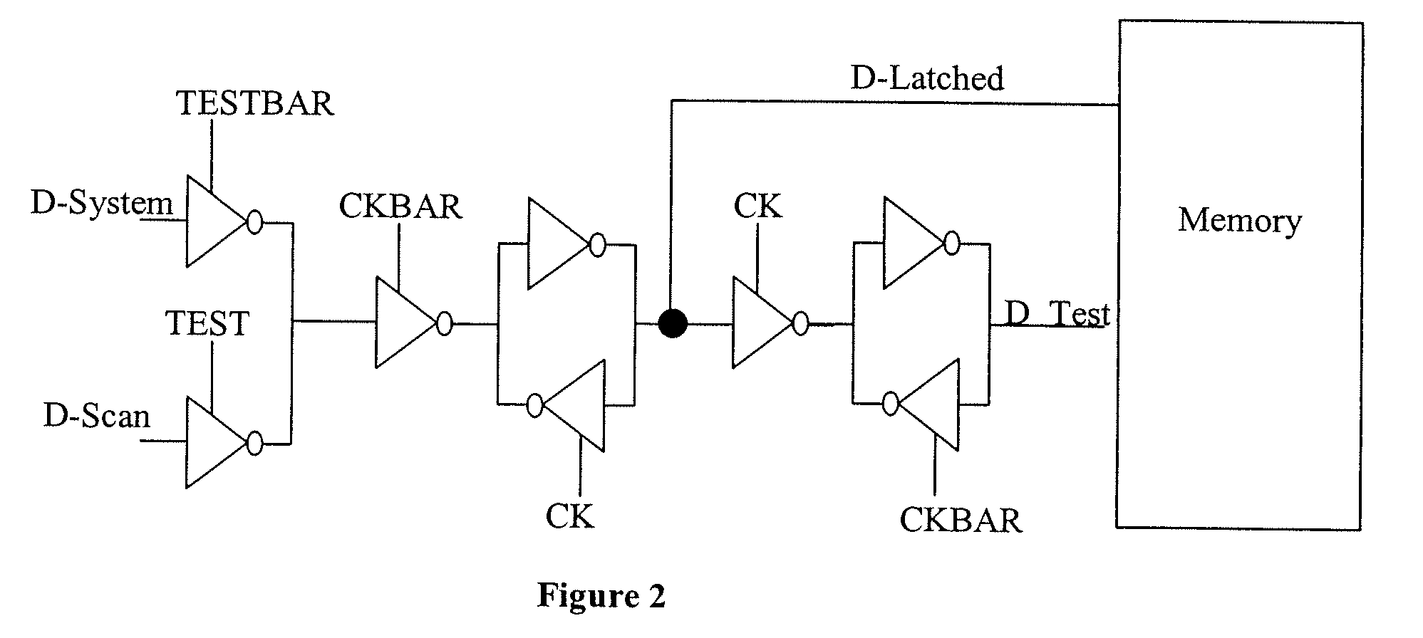
[0017] The instant invention is directed generally to or targets a new high-speed interface for testing and debugging the embedded memories. This interface does not change the timing of the Inputs / Outputs or the memory and may be seamlessly integrated into the original memory Inputs / Outputs. One basic idea behind such an interface is first to use the latch on the memory input, and subsequently to convert the latch to a scan flip-flop.

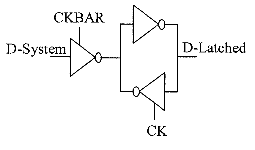
[0018]FIG. 1 shows a schematic diagram of a latch in accordance with an embodiment of the present invention. As illustrated in the figure, the latch comprises a tri-state inverter connected to a test input signal, D-system. A test control signal, CKBAR, is applied to a tri-state inverter. The output of the tri-state inverter is fed to a pair of logical elements connected in a closed loop. The pair of logical elements includes a logic inverter and a tri-state inverter connected in series. The tri-state inverter receives a control signal, CK, which is th...


PUM


Abstract

An integrated scannable interface for testing memory. The interface includes a selection device for selecting a signal from at least two input signals responsive to an activation signal, a first storage device coupled to the output of the selection device for storing the signal responsive to a first enable signal and generating an output signal for the memory. The first storage device is connected at the input node of the memory, and a second storage device is coupled at its input to the first storage device for storing the output signal responsive to a second enable signal and generating a test signal for testing the memory. The output signal is observed for debugging faults between the integrated scannable interface and the memory and for debugging faults between the first and second storage devices.

Description

Related Application [0001] The present application claims priority of India Patent Application No. 1512 / Del / 2005 filed Jun. 10, 2005, which is incorporated herein in its entirety by this reference. FIELD OF THE INVENTION [0002] The present invention relates to an integrated interface to test and debug failing memory on an integrated circuit. BACKGROUND OF THE INVENTION [0003] The increasing complexity on chip and of chip designs is inducing more defects in System on Chip (SoC) designs, and these defects are causing an increase in the testing requirements for each chip. [0004] The yield of SOC and their designs is directly linked to the memories on the SOC because there are around 60 to 70 percent of the memories on the chip. Thus, the memory yield is directly converted to or related to the chip yield. A robust design and a very well controlled process can reduce the defect level in the memory, but, unfortunately in the newer technologies, as the gate lengths shrink, the defect level...

Claims


Application Information

Patent Timeline
Patent Type & Authority Applications(United States)
IPC IPC(8): G01R31/28
CPCG01R31/318533G11C29/02G11C29/022G11C2029/3202G11C29/48G11C29/50012G11C2029/0401G11C29/1201
Inventor DUBEY, PRASHANT
Owner STMICROELECTRONICS PVT LTD
Features
  • R&D
  • Intellectual Property
  • Life Sciences
  • Materials
  • Tech Scout
  • Unparalleled Data Quality
  • Higher Quality Content
  • 60% Fewer Hallucinations
Learn More