Fast systems and methods for calculating electromagnetic fields near photomasks

a technology of electromagnetic fields and systems, applied in the field of masks, can solve the problems of accompanied by unwanted distortions and artifacts, methods are typically considered too slow to be used on a full reticle scale, and the approximation is much less accura

Inactive Publication Date: 2007-01-11
LUMINESCENT TECH
View PDF3 Cites 24 Cited by
  • Summary
  • Abstract
  • Description
  • Claims
  • Application Information

AI Technical Summary

Benefits of technology

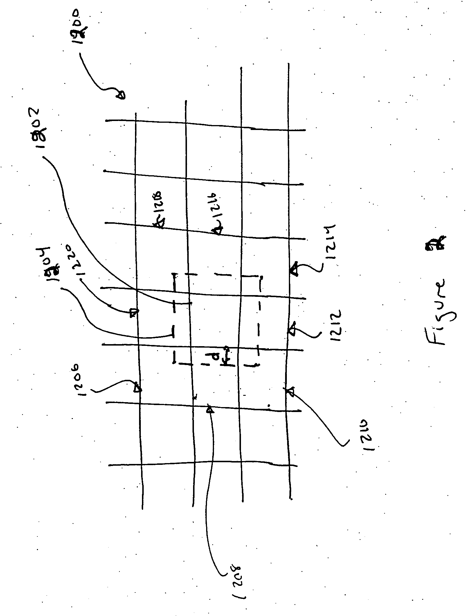
[0013] Aspects may provide for blocks to be processed using any of the methods described above. In some embodiments, blocks may be processed in parallel using multiple processors, blades or accelerator cards. Aspects may provide for the blocks to be combined after processing to provide an electromagnetic field representation for an entire layer of a semiconductor device or other workpiece. These aspects may provide for efficient full chip calculation of an electromagnetic field.

Problems solved by technology

However, due to the wave nature of light, as dimensions approach sizes comparable to the wavelength of the light used in the photolithography process, the resulting wafer patterns deviate from the corresponding photomask patterns and are accompanied by unwanted distortions and artifacts.
Although the Kirchoff model is reasonably accurate for large features, the approximation is much less accurate as the mask features become comparable to the wavelength of light.
Unfortunately, such methods are typically considered too slow to be used on a full reticle scale.

Method used


Image

  • Fast systems and methods for calculating electromagnetic fields near photomasks
  • Fast systems and methods for calculating electromagnetic fields near photomasks
  • Fast systems and methods for calculating electromagnetic fields near photomasks

Examples


Embodiment Construction

[0021] In order to calculate a representation of an electromagnetic field, we begin with a description of the pattern on the photomask. A function ψ(x, y) may represent an example photomask pattern by defining the contours which enclose the regions in photomask pattern. ψ(x, y) can be a function which defines the contours implicitly in the sense that a two dimensional function is used to describe a set of contours. Frequently, the function ψ(x, y) is thought of as a real-valued function that defines the contour according to the value of the function along the contour. For example, in one embodiment the mask function ψ(x, y) has the property that ψ(x, y)

[0022] 1. ψ(x, y)=0 everywhere along the boundary of a region;

[0023] 2. ψ / (x, y)>0 “inside” a region (for example, those regions corresponding to the chrome portions of the mask);

[0024] 3. ψ(x, y)<0, or is negative “outside” a region (for example, those regions corresponding to the clear quartz portions of the mask).

[0025] In this...


PUM

PropertyMeasurementUnit
sizeaaaaaaaaaa
sizeaaaaaaaaaa
sizeaaaaaaaaaa

Abstract

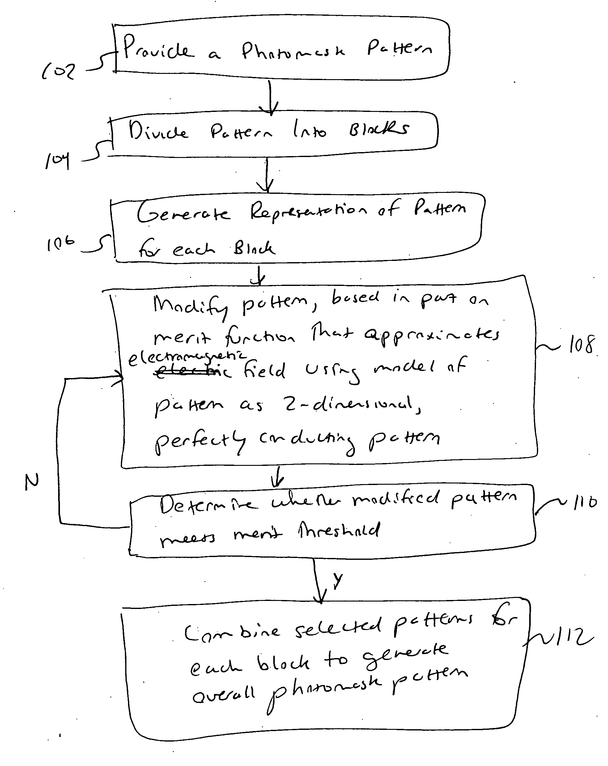
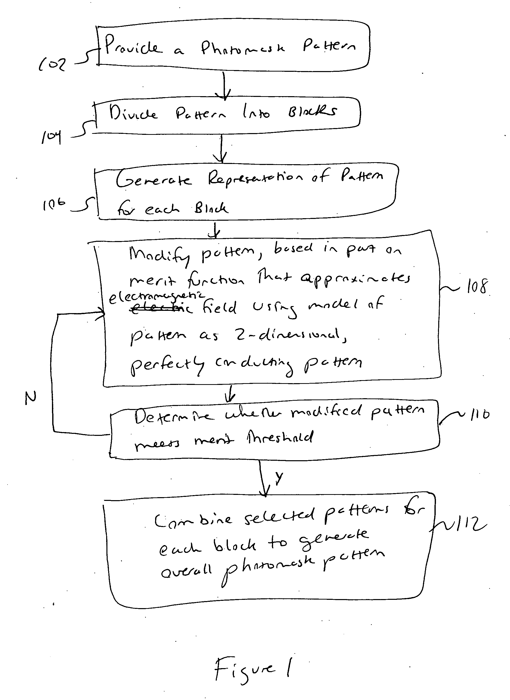
Photomask patterns are represented using contours defined by mask functions. Given target pattern, contours are optimized such that defined photomask, when used in photolithographic process, prints wafer pattern faithful to target pattern. Optimization utilizes “merit function” for encoding aspects of photolithographic process, preferences relating to resulting pattern (e.g. restriction to rectilinear patterns), robustness against process variations, as well as restrictions imposed relating to practical and economic manufacturability of photomasks. Merit function may approximate electromagnetic field using model of mask pattern as infinitely thin, perfectly conducting pattern. Model may also be used for other lithographic methods, including simulation and verification.

Description

CROSS-REFERENCE [0001] This application claims the benefit of U.S. Provisional Application No. 60 / 616,789 filed on Oct. 6, 2004, which is incorporated herein by reference in its entirety.FIELD OF INVENTION [0002] Field relates to masks, also known as photomasks, used in photolithography processes and, more particularly, to systems and-methods for calculating the electromagnetic fields near a photomask. DESCRIPTION OF RELATED ART [0003] Lithographic techniques are used to define patterns, geometries, features, shapes, et al (“patterns”) onto an integrated circuit die or semiconductor wafer or chips where the patterns are typically defined by a set of contours, lines, boundaries, edges, curves, et al (“contours”), which generally surround, enclose, and / or define the boundary of the various regions which constitute a pattern. [0004] Demand for increased density of features on dies and wafers has resulted in the design of circuits with decreasing minimum dimensions. However, due to the ...

Claims


Application Information

Patent Timeline
Patent Type & Authority Applications(United States)
IPC IPC(8): G06F17/50G03F1/00G21K5/00G03F1/36
CPCG03F1/144G03F7/705G03F1/36
Inventor ABRAMS, DANIEL S.
Owner LUMINESCENT TECH
Why Eureka
Try Eureka