MEMS packaging method for enhanced EMI immunity using flexible substrates

a flexible substrate and packaging method technology, applied in the field of packaging mems devices and mems packages, can solve the problems of distorting the sensitivity and the performance of the mems device, packaging is the biggest challenge for commercializing most mems devices, and the packaging is the biggest challenge for most mems devices

Active Publication Date: 2007-01-18
SHANDONG GETTOP ACOUSTIC
View PDF7 Cites 130 Cited by
  • Summary
  • Abstract
  • Description
  • Claims
  • Application Information

AI Technical Summary

Benefits of technology

[0015] A principal object of the present invention is to provide an effective and very manufacturable method of producing a MEMS package incorporating a MEMS device and one or more other electronic circuits.

Problems solved by technology

However, packaging of a MEMS device is totally different from packaging an integrated circuit.
Packaging is the biggest challenge for commercializing most MEMS devices.
For example, the packaging stress can distort the sensitivity and the performance of the MEMS devices.
MEMS devices include delicate movable structures which are easily damaged through fabrication and assembly processes.
As such, the assembly yield of a MEMS package is often a challenging target to meet.
The packaging requirements of MEMS devices are complex because the devices need to interact with the physical phenomenon and yet the devices need to be protected from the environment.
However, interconnecting the two substrates is a challenging task.
However, ubiquitous electromagnetic interference (EMI) leakage is a major noise source to most electronic devices, especially for acoustic MEMS devices because of required openings for sound inlet.

Method used


Image

  • MEMS packaging method for enhanced EMI immunity using flexible substrates
  • MEMS packaging method for enhanced EMI immunity using flexible substrates
  • MEMS packaging method for enhanced EMI immunity using flexible substrates

Examples


first embodiment

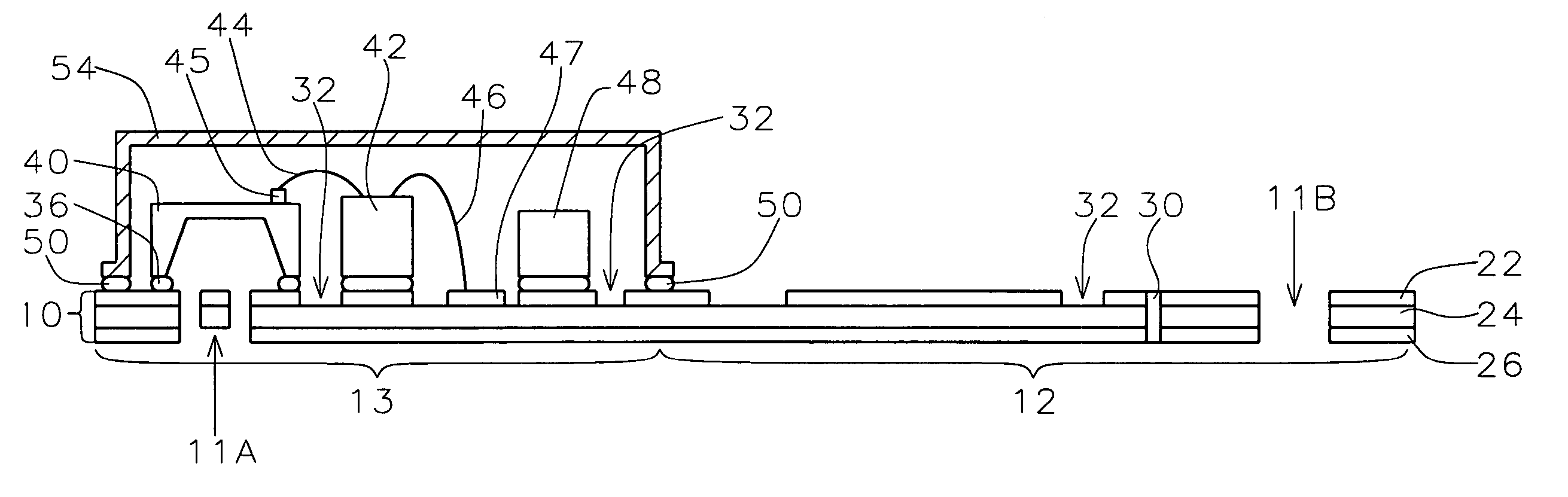
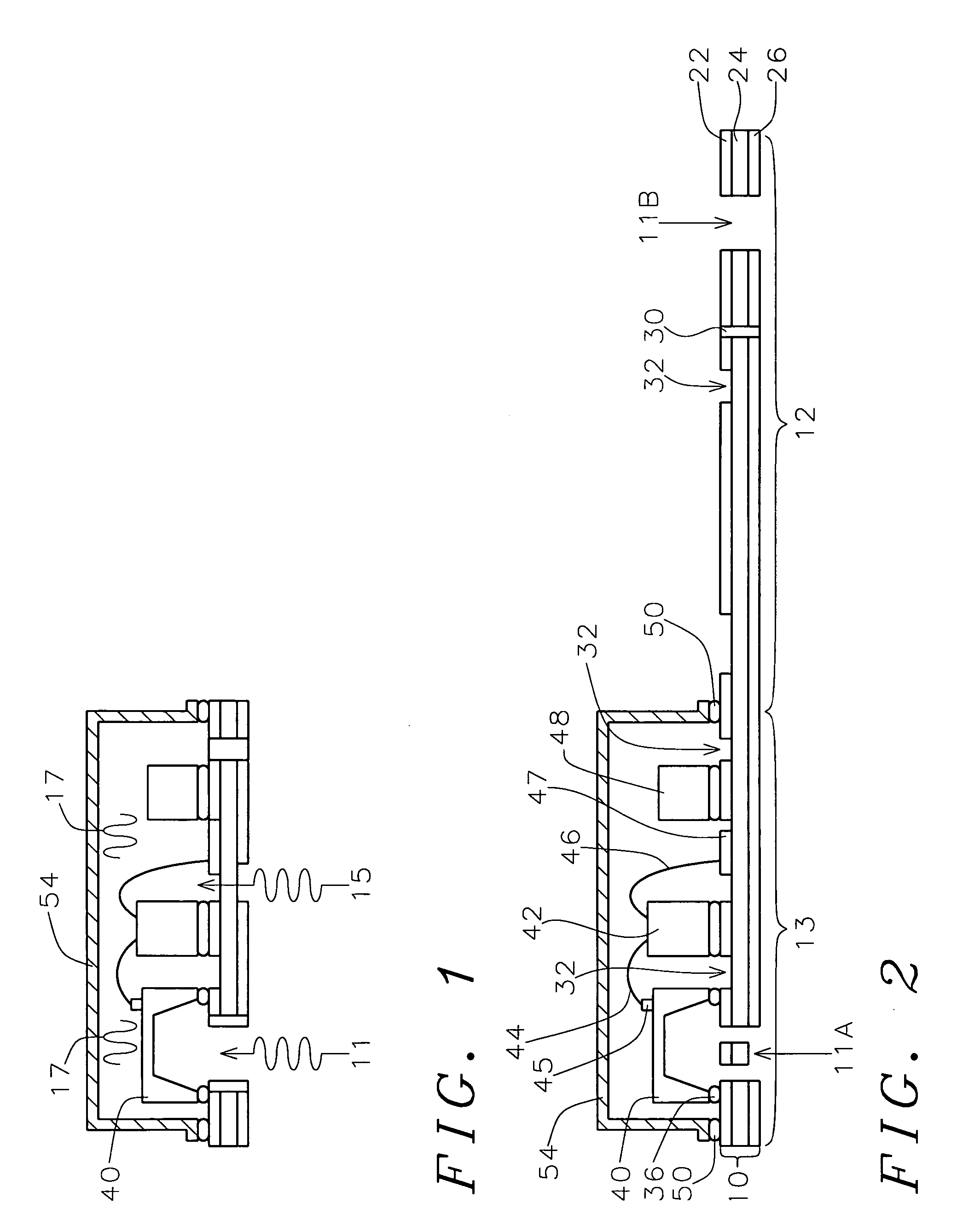
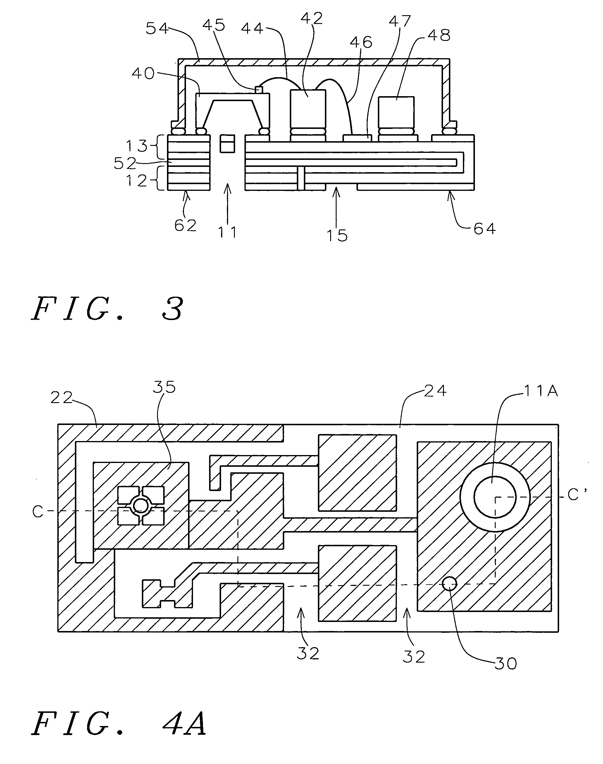
[0050] the invention will now be described with reference to FIGS. 2 through 6. Referring now more particularly to FIG. 2, there is illustrated a double metal layer (2ML) flexible substrate of the present invention. The flexible substrate 10 is formed of the core film layer 24 and copper metal layers 22 and 26 on both sides. The core film layer may be polyimide, polyethylene polyimide (PEI), poly tetra fluoro ethylene (PTFE), or liquid crystal polymer (LCP).). The polyimide layer 24 is between about 12.5 and 100 μm in thickness. Such a core film of the flexible substrate 10 has a much lower modulus (typically 5 GPa) than a FR-4 printed circuit board (PCB) (typically 25 GPa), and so offers stress relaxation and minimizes the interaction of packaging stress or environmentally induced stress with a MEMS device mounted on it. The flexible substrate 10 includes a portion 13 on which are mounted the devices and an elongated portion 12.

[0051] Metal layers 22 and 26 are laminated to the top...

second embodiment

[0064] the present invention will be described with reference to FIGS. 10-14. In this embodiment, a rigid conductive plate is combined with a flexible substrate of the invention. In this embodiment, a single metal layer (1ML) flexible substrate 10 may be used. Referring now to FIG. 10, a 1ML flexible substrate 10 is illustrated, comprising metal layer 22 and core film 24. The core film layer may be polyimide, polyethylene polyimide (PEI), poly tetra fluoro ethylene (PTFE), or liquid crystal polymer (LCP).). The polyimide layer 24 is between about 12.5 and 100 μm in thickness. The flexible substrate 10 includes a portion 13 on which are mounted the devices and an elongated portion 12.

[0065] Metal layer 22 is laminated to the top of the flexible core film layer 24 using adhesive or adhesive-less laminating techniques. Metal layer 22 is preferably copper, having a metal surface finish for wirebonding. The copper layer is typically 25 μm in thickness, but can be more or less, depending ...


PUM


Abstract

A MEMS package and methods for its embodiment are described. The MEMS package has at least one MEMS device mounted on a flexible and foldable substrate. A metal cap structure surrounds the at least one MEMS device wherein an edge surface of the metal cap structure is attached to the flexible substrate and wherein a portion of the flexible substrate is folded under itself thereby forming the MEMS package. A meshed metal environmental hole underlying the at least one MEMS device provides enhanced EMI immunity.

Description

[0001] This is a Continuation-in-Part of U.S. patent application (AL05-001) Ser. No. 11 / 182,254, filed on Jul. 15, 2005, which is herein incorporated by reference in its entirety.BACKGROUND OF THE INVENTION [0002] (1) Field of the Invention [0003] The invention relates to processes for packaging MEMS devices, and MEMS packages produced using the method, and more particularly, to a method of packaging MEMS devices for enhanced EMI immunity using a flexible, foldable substrate. [0004] (2) Description of the Related Art [0005] Micro-electro-mechanical systems (MEMS) devices are known which convert physical phenomena, such as pressure, acceleration, sound, or light, into electrical signals. Each type of MEMS device interacts with the world in a different way, and demands custom or at least semi-custom packaging solutions. So-called system-in-package techniques attempt to form an entire microsystem—which could include a microprocessor, communications components, actuators and sensors—wit...

Claims


Application Information

Patent Timeline
Patent Type & Authority Applications(United States)
IPC IPC(8): H01L23/12
CPCB81B2201/0257H01L2924/07802B81C1/00309H01L23/057H01L23/5387H01L23/552H01L2224/32225H01L2224/48091H01L2224/48137H01L2224/48227H01L2224/49109H01L2224/73265H01L2924/01077H01L2924/01078H01L2924/01079H01L2924/09701H01L2924/1433H01L2924/15311H01L2924/16152H01L2924/19041H01L2924/19105H01L2924/3025B81C1/0023H01L2924/01322H01L2924/01087H01L2924/01019H01L2924/1461H01L24/48H01L24/49H01L2924/00014H01L2924/00H01L2924/00012H01L2224/451H01L24/73H01L2924/14H01L2224/05554H01L2924/15151H01L2924/181H01L2224/45099H01L2224/05599B81B3/00H01L23/12
Inventor ZHE, WANGYUBO, MIAO
Owner SHANDONG GETTOP ACOUSTIC
Why Eureka
Try Eureka