Display device

a display device and display technology, applied in the direction of discharge tube luminescnet screens, discharge tube/lamp details, cathode ray tubes/electron beam tubes, etc., can solve the problems of difficult to specify the discharge location, reduced service life of the panel, emission, etc., to achieve excellent effect, greatly enhanced service life of the display device, and inhibit the effect of luminance deterioration

Inactive Publication Date: 2007-01-18
HITACHI DISPLAYS
View PDF4 Cites 1 Cited by
  • Summary
  • Abstract
  • Description
  • Claims
  • Application Information

AI Technical Summary

Benefits of technology

[0017] According to the display device according to the invention, as discharge is easily caused between the positive electrode and the conductive metallic film in the structure, discharge is hardly caused between the electron emission element and the positive electrode in normal operation and the breakdown of the electron emission element can be inhibited. As gas can be prevented from being caused by the breakdown of the electron emission element, the deterioration of luminance can be inhibited. Therefore, extremely excellent effect that the service life of the display device is greatly enhanced and the reliable display device having high quality can be realized is acquired.
[0018] Besides, according to the display device according to the invention, as a knocking process is performed in a manufacturing process between the positive electrode and the conductive metallic film and discharge is forcedly caused, discharge in normal operation can be controlled. Further, as locations where discharge is easily caused in the operation can be reduced by knocking, extremely excellent effect that a service life of the display device can be extended is acquired.

Problems solved by technology

When discharge is caused, a problem that the service life of a panel is reduced and emission occurs in a location except a predetermined location occurs.
However, as discharge is caused in a location in which contact between the spacer and the electrode is imperfect, there is a problem that it is difficult to specify the location of discharge.

Method used


Image

  • Display device
  • Display device
  • Display device

Examples


first embodiment

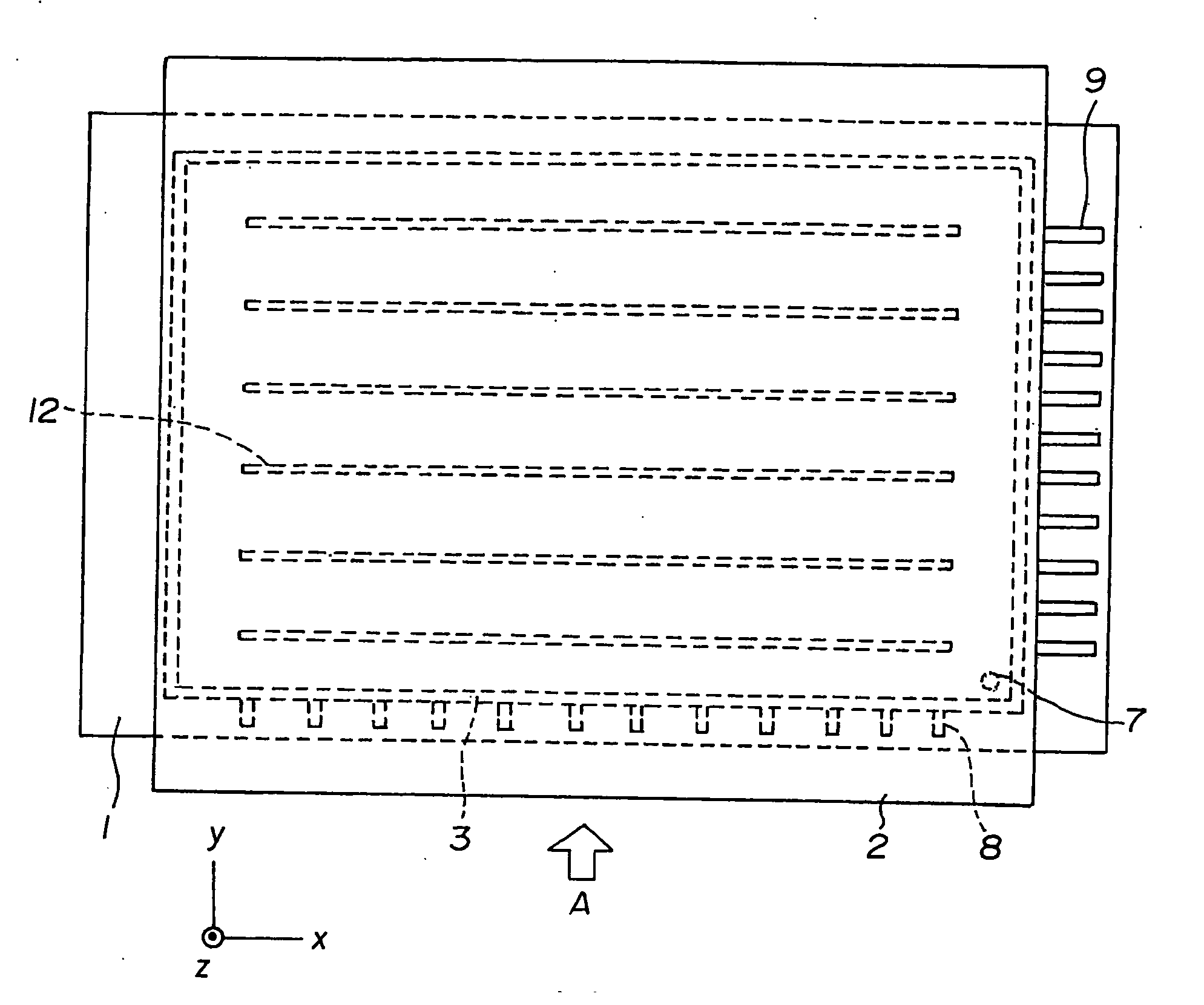
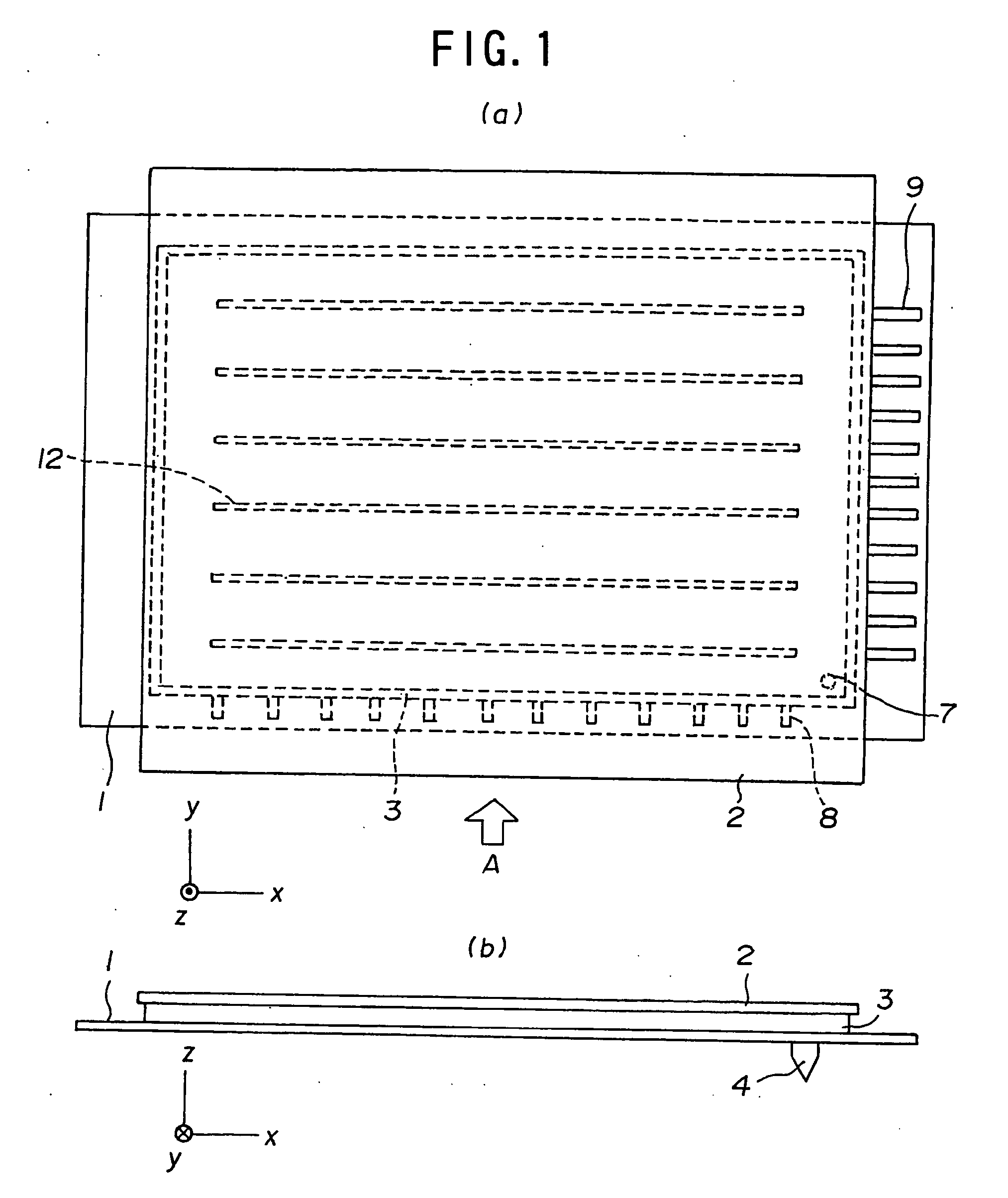
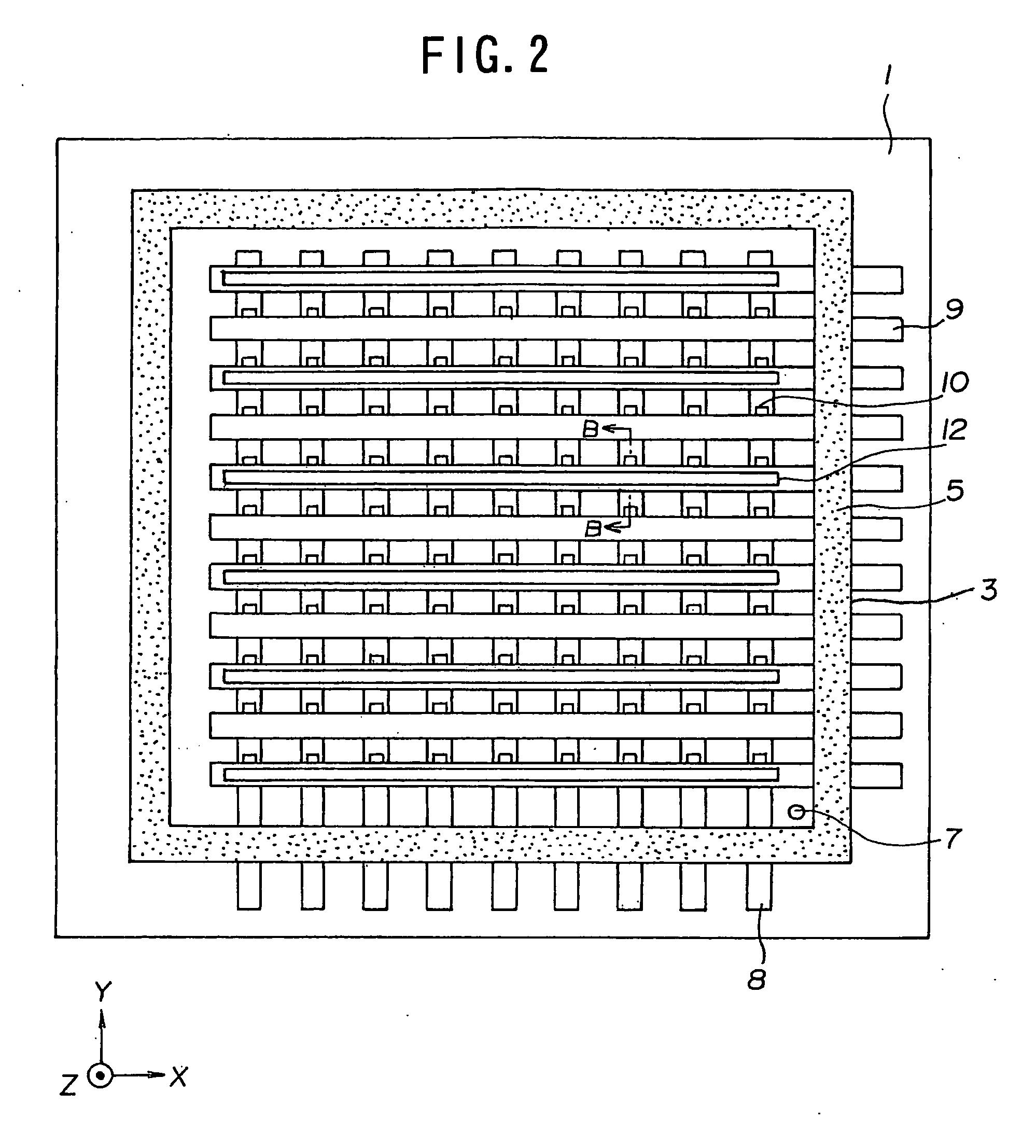
[0034]FIGS. 1A, 1B and 2 are explanatory drawings for explaining the configuration in a first embodiment of a display device according to the invention, where FIG. 1A is a plan showing the display device viewed from the side of a front board, FIG. 1B is a side view viewed from a direction shown by an arrow A in FIG. 1A, and FIG. 2 is a schematic plan showing a back board of the display device from which the front board shown in FIGS. 1A and 1B is removed. FIG. 3 is a schematic enlarged sectional view showing the back board viewed along a line B-B shown in FIG. 2 and the front board in a corresponding part to the back board.

[0035] As shown in FIGS. 1A to 3, a reference numeral 1 denotes the back board, 2 denotes the front board, and these back board 1 and front board 2 are made of a glass plate a few mm in thickness, for example approximately 3 mm. A reference numeral 3 denotes a frame and the frame 3 is made of a glass plate or a sintered body of fritted glass a few mm in thickness...

second embodiment

[0048]FIGS. 7 and 8 are explanatory drawings for explaining the configuration of a spacer in a second embodiment of the display device according to the invention in detail, FIG. 7 is a plan viewed from the side of the spacer, and FIG. 8 is a sectional view viewed along a line II-II shown in FIG. 7. In these drawings, the same reference numeral is allocated to the same part as that in the above-mentioned drawings and the description is omitted.

[0049] The spacer 12 used in this display device is formed in a shape of a thin plate by an insulating material such as ceramic material. A conductive metallic film 13 is coated on both side walls of a base of the spacer by sputtering or depositing metallic material such as Al, Cr, Ni, Mo, Ta and Cu for example. The specific resistance of the base of the spacer 12 is approximately 108 to 109 Ω·cm.

[0050] The conductive metallic film 13 is formed in an overall area having a fixed height from the side end of a back board toward the side of a fro...

third embodiment

[0061]FIG. 11 is a plan viewed from the side of a spacer for explaining the configuration of the spacer in a third embodiment of the display device according to the invention in detail, the same reference numeral is allocated to the same part as that in the above-mentioned drawings, and the description is omitted.

[0062] The spacer 12 used in a display device is formed in the shape of a thin plate by an insulating material such as ceramic material. A conductive metallic film 13 is coated on both side walls of a base of the spacer in an overall area in a longitudinal direction by sputtering or depositing metallic material such as Al, Cr, Ni, Ta, Mo and Cu. Further, irregularities 13c are integrated on the side of a front board of the conductive metallic film 13.

[0063] The surface electrical resistance of the conductive metallic film 13 is set to 106Ω / □ or less on the side of the base of the spacer 12. The height HC of the conductive metallic film 13 is equivalent to ⅕ to 1 / 100 of th...


PUM


Abstract

The object of the invention is to provide a display device, particularly to provide a display device that inhibits discharge caused in the operation of the display device utilizing field emission and enables image display for a long time. Discharge between a metal-backed film and an electron emission element is inhibited by forming a plurality of spacers arranged in a display area between a front board and a back board by an insulating material, providing a conductive metallic film on side walls of the spacer and integrating a convex portion protruded on the side of the front board with the conductive metallic film.

Description

CLAIM OF PRIORITY [0001] The present application claims priority from Japanese Application JP 2005-206694 filed on Jul. 15, 2005, the content of which is hereby incorporated by reference into this application. FIELD OF THE INVENTION [0002] The present invention relates to a display device, in particular, it relates to a display device provided with plural gap holding members between opposite faces of a front board on which a fluorescent screen is formed and a back board on which an electron emission element is formed, and detailedly relates to a discharge measure structure of the gap holding member. BACKGROUND OF THE INVENTION [0003] A display device for making a fluorescent screen emit light by colliding an electron with the fluorescent screen and displaying an image includes a thin cathode ray tube provided with a cold cathode represented by a field emission display provided with a field emission type electron source and a surface conduction display provided with a surface conduct...

Claims


Application Information

Patent Timeline
Patent Type & Authority Applications(United States)
IPC IPC(8): H01J1/62
CPCH01J29/864H01J31/127H01J2329/866H01J2329/8645H01J2329/8655H01J2329/864
Inventor HIRASAWA, SHIGEMIKATO, KENJISHINTANI, HIDEYUKI
Owner HITACHI DISPLAYS
Why Eureka
Try Eureka