Semiconductor device and manufacturing method thereof

Inactive Publication Date: 2007-01-18
SHINKO ELECTRIC IND CO LTD
View PDF14 Cites 12 Cited by
  • Summary
  • Abstract
  • Description
  • Claims
  • Application Information

AI Technical Summary

Benefits of technology

[0040] In addition, since the first substrate is a silicon substrate, the transfer of heat can be excellent.
[0041] According to embodiments of the present invention, a semiconductor device and a manufacturing method

Problems solved by technology

For example, an LED emits a predetermined color light; however, the kinds of colors are limited.
However, a semiconductor device in which a substrate on which an LED is mounted is further mounted on another substrate is not disclosed.
In the above described semiconductor device, in some cases, a defective semiconductor device is manufactured caused by, for example, irregular color and poor light emission due to an individual difference o

Method used


Image

  • Semiconductor device and manufacturing method thereof
  • Semiconductor device and manufacturing method thereof
  • Semiconductor device and manufacturing method thereof

Examples


first embodiment

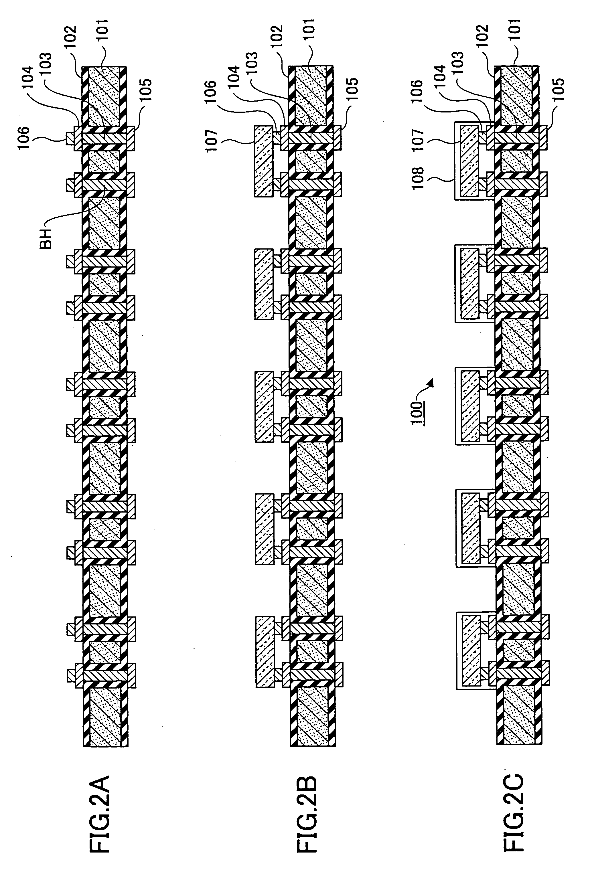
[0050]FIGS. 2A through 2F are schematic cross-sectional views showing processes in a manufacturing method of a semiconductor device according to a first embodiment of the present invention.

[0051] Referring to FIGS. 2A through 2F, the manufacturing method of the semiconductor device according to the first embodiment of the present invention is described.

[0052] In the following description, the manufacturing method for one semiconductor device is mainly explained; however, the number of the semiconductor devices is not limited to one, and plural semiconductor devices are actually formed at the same time.

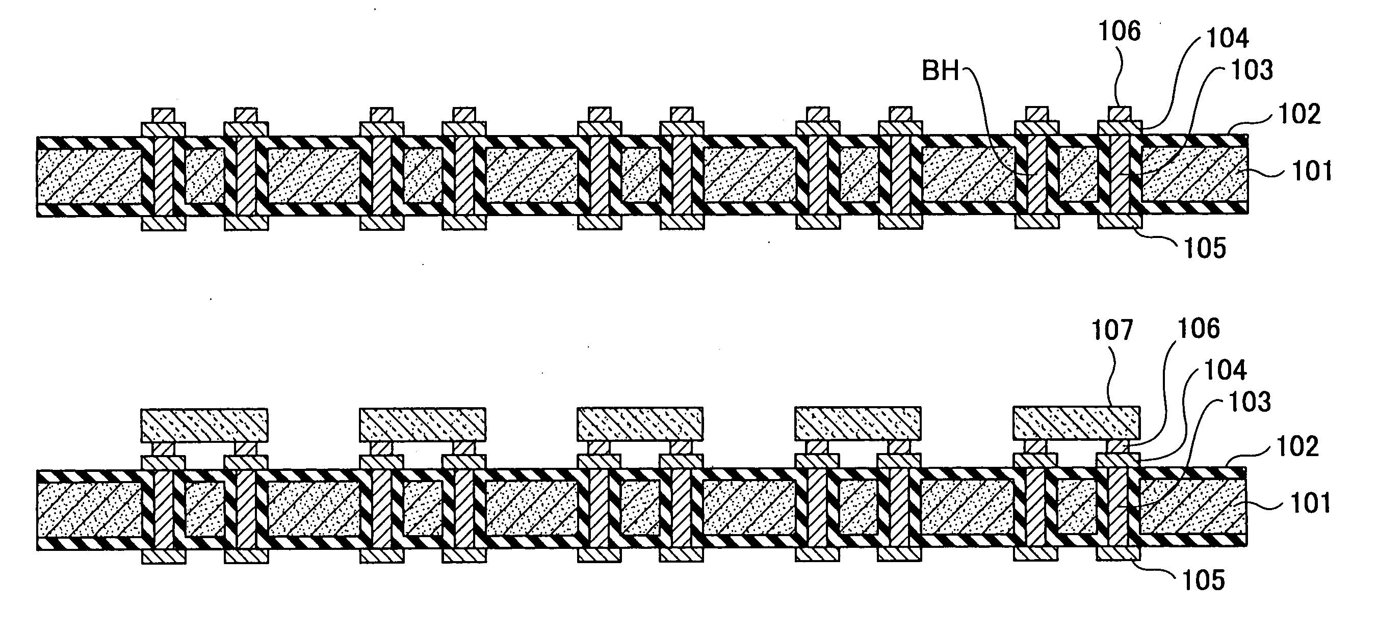
[0053] First, in a process shown in FIG. 2A, via holes BH are formed in a substrate 101 made of, for example, a silicon wafer, and an insulation layer 102 is formed on the surface of the substrate 101 and on the inner wall surface of the via holes BH. The insulation layer 102 can be formed by various methods. For example, a film of an organic material such as a resin material is for...

second embodiment

[0085] Next, a second embodiment of the present invention is described. In the second embodiment, the first embodiment is modified. FIG. 3 is a schematic cross-sectional view showing a semiconductor device 200A according to the second embodiment of the present invention. As shown in FIG. 3, the semiconductor device 200A includes a substrate 101A made of, for example, silicon on which a semiconductor element 107A is mounted, and a substrate 201A made of, for example, a ceramic material on which the substrate 101A is mounted.

[0086] The semiconductor element 107A is similar to the semiconductor element 107 in the first embodiment and has a structure similar to the structure of the semiconductor element 107. Further, an optical function layer 108A similar to the optical function layer 108 in the first embodiment is formed on the semiconductor element 107A.

[0087] A concave section 204A which contains the substrate 101A on which the semiconductor element 107A is mounted is formed in the...

third embodiment

[0097] Referring to FIG. 5, a semiconductor device according to a third embodiment of the present invention is described. FIG. 5 is a schematic cross-sectional view showing a semiconductor device 200B according to the third embodiment of the present invention. As shown in FIG. 5, the semiconductor device 200B includes a substrate 101B made of, for example, silicon on which a semiconductor element 107B is mounted, and a substrate 201B made of, for example, a ceramic material on which the substrate 101B is mounted.

[0098] The semiconductor element 107B is similar to the semiconductor element 107 in the first embodiment and has a structure similar to the structure of the semiconductor element 107. The semiconductor element 107B is mounted on the substrate 101B so that the semiconductor element 107B is contained in a concave section 111 formed in the substrate 101B. The concave section 111 is formed as an approximate rectangular parallelopiped shape or an approximate cylindrical shape b...


PUM


Abstract

A manufacturing method of a semiconductor device is disclosed. The manufacturing method includes a first step that mounts plural semiconductor elements on a first substrate, a second step that inspects each of the semiconductor elements mounted on the first substrate, a third step that divides the first substrate by dicing so that a divided first substrate includes at least one semiconductor element, and a fourth step that mounts the divided first substrate in which at least one semiconductor element is mounted on a second substrate.

Description

BACKGROUND OF THE INVENTION [0001] 1. Field of the Invention [0002] The present invention generally relates to a semiconductor device and a manufacturing method thereof in which a substrate on which a semiconductor element is mounted is further mounted on another substrate. [0003] 2. Description of the Related Art [0004] There are various kinds of semiconductor devices on which a semiconductor element is mounted. For example, when the semiconductor element is an optical function element having a light emitting function or a photoelectric conversion function, the semiconductor device can be used as a displaying device, a communicating device, a measuring device, a controlling device, and so on. Such a semiconductor device is formed by mounting an optical function element on a predetermined substrate on which wirings are formed. [0005]FIGS. 1A through 1C are schematic cross-sectional views showing processes for manufacturing a semiconductor device on which an LED (light emitting diode...

Claims


Application Information

Patent Timeline
IPC IPC(8): H01L21/00H01L33/60H01L33/50H01L33/62
CPCH01L25/0753H01L33/486H01L2924/10253H01L2224/73265H01L2224/48091H01L2224/16145H01L2924/19107H01L2924/15311H01L2224/73204H01L2224/32225H01L24/97H01L2224/16225H01L2924/12041H05K2201/10106H05K1/183H01L2933/0041H01L33/50H01L33/62H01L2924/00H01L2924/00014
Inventor SHIRAISHI, AKINORIHIGASHI, MITSUTOSHITAGUCHI, YUICHI
Owner SHINKO ELECTRIC IND CO LTD
Why Eureka
Try Eureka