Optimized multi-apparation assembly

a multi-apparation, assembly technology, applied in the direction of electrical apparatus, semiconductor devices, semiconductor/solid-state device details, etc., can solve the problems of drawbacks and limitations regarding the quality of miniaturization and the implementation of such an assembly in complex systems

Inactive Publication Date: 2007-01-25
NXP BV
View PDF5 Cites 15 Cited by
  • Summary
  • Abstract
  • Description
  • Claims
  • Application Information

AI Technical Summary

Benefits of technology

[0022] Such a method allows a very compact system presenting the same functionalities than a larger one if realized by other techniques like integration on a single chip. Therefore, such a method avoids an integration of devices of different kinds on a same chip. The different chips are effectively realized independently and then assembled according to the invention.

Problems solved by technology

The assembly proposed in this prior art document therefore presents drawbacks and limitation regarding the quality of the miniaturization and the implementation of such an assembly for complex systems.

Method used


Image

  • Optimized multi-apparation assembly
  • Optimized multi-apparation assembly
  • Optimized multi-apparation assembly

Examples


Embodiment Construction

[0028] The terms ‘top’ and ‘bottom’ are used herein to indicate directions relative to the structure of the microelectronic chip assembly itself or to a connection device. It should be understood that these terms are used to refer to the frame of reference of the assembly itself or to said connection device, and not to the ordinary, gravitational frame of reference.

[0029] The term ‘device’ designates any component, function, circuit, application that can be integrated on a microelectronic chip.

[0030] The term ‘system’ designates any combination of electronic functions to perform a complete application, excluding a single integrated circuit (IC).

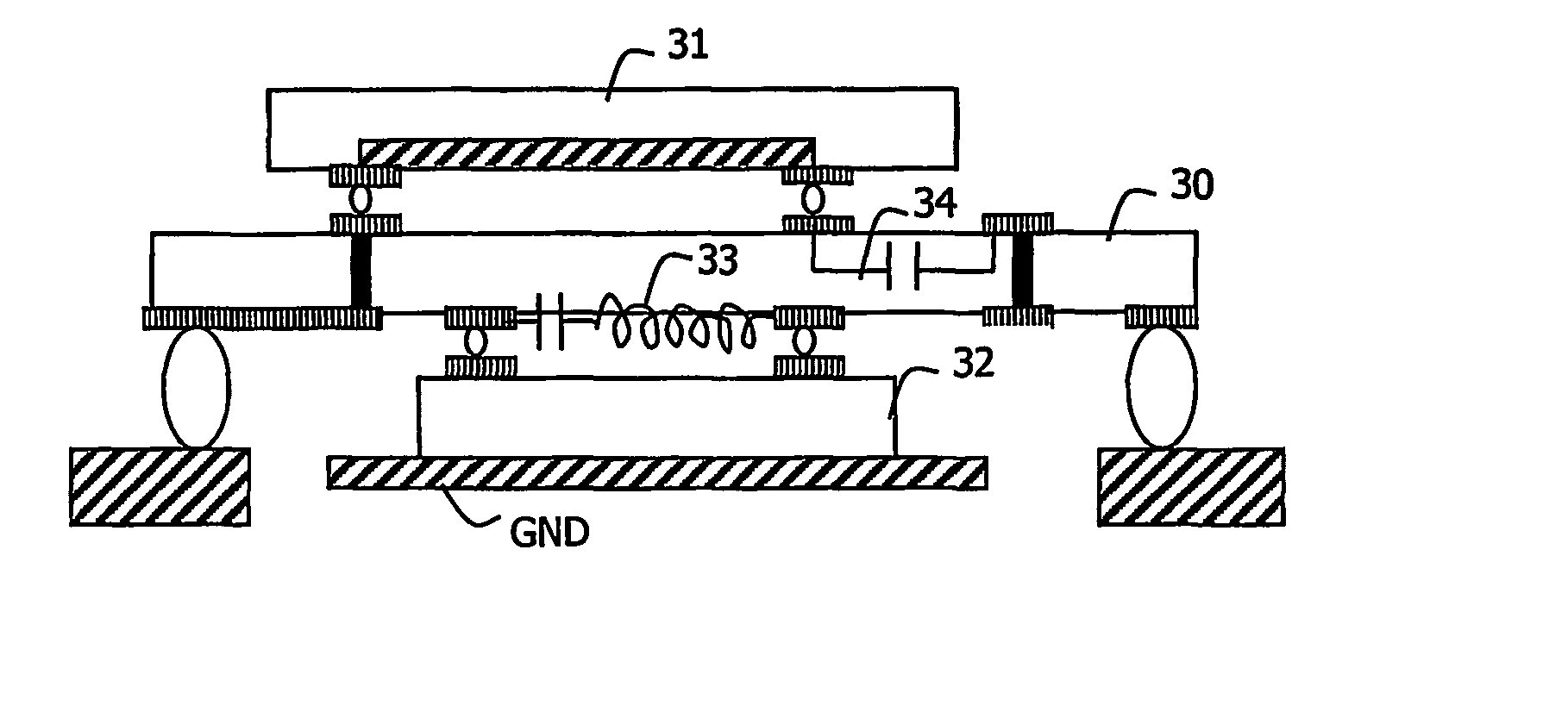
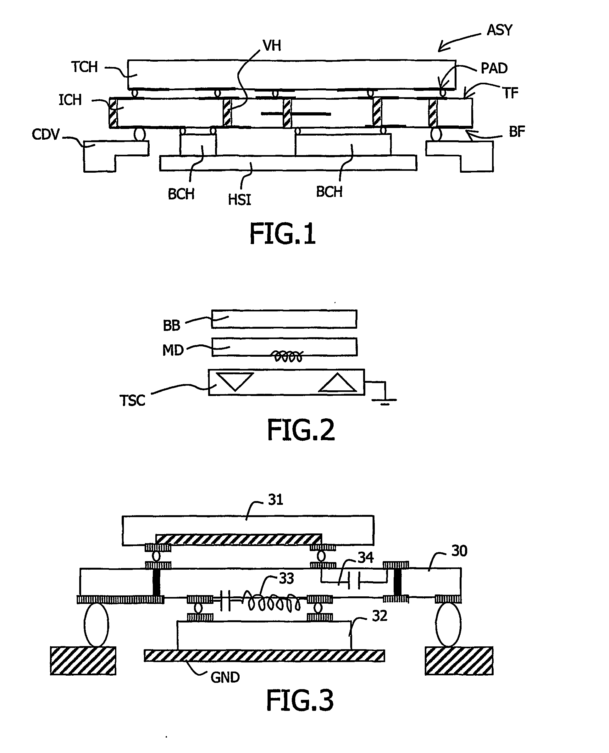
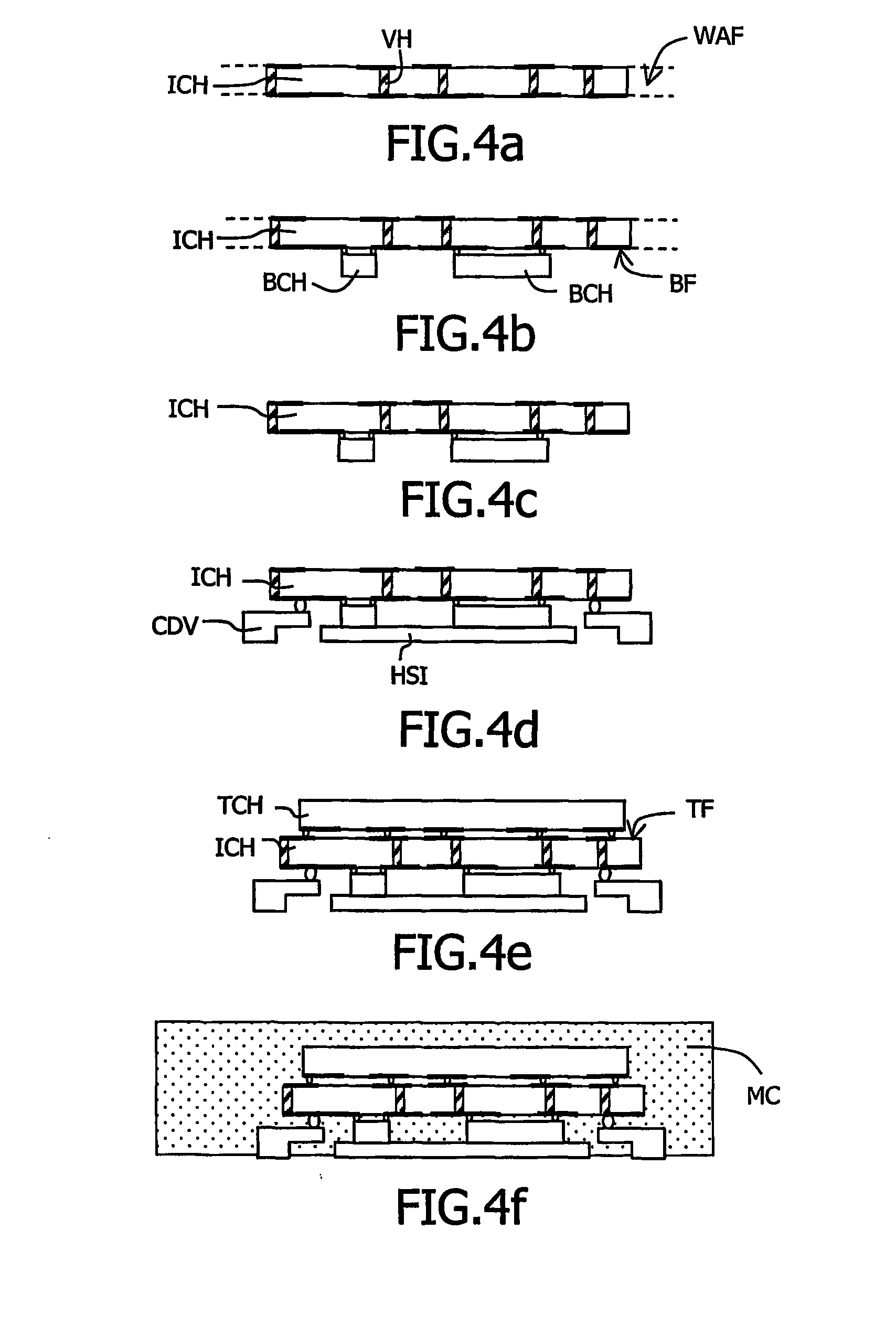
[0031]FIG. 1 represents a microelectronic chip assembly ASY according to the invention. This assembly includes three microelectronic chips TCH, ICH, BCH on which integrated devices are formed. Integrated devices are integrated using semi-conductor or semi-insulating technologies.

[0032] Bolder lines on this Figure symbolize terminal pads P...


PUM


Abstract

The invention relates to a microelectronic chip assembly ASS comprising at least three microelectronic chip ICH, TCH, BCH stacked together and on which integrated devices are formed. At least one of the chip, called intermediate chip ICH, includes via holes VH running through said chip ICH and filled with conductive material is realized from a high-ohmic substrate on which are formed devices for the functioning of at least two other microelectronic chips, called top chip TCH and bottom chip BCH. Said top and bottom chips TCH and BCH are connected by flip chip bonding respectively on top face TF and bottom face BF of said intermediate chip ICH and said via holes VH are electrically connected to pads of said top and bottom chips TCH and BCH.

Description

FIELD OF THE INVENTION [0001] This invention relates to the field of electronic system packaging. More particularly the invention relates to assembly incorporating at least three microelectronic chips on which integrated devices are formed, said chips being stacked together and at least one of the chips including via holes running through said chip and filled with conductive material. The invention also relates to a microelectronic chip intended to be used in such an assembly and to a packaged system including at least such an assembly. Finally, the invention relates to a method of manufacturing such an assembly. BACKGROUND OF THE INVENTION [0002] Such an assembly is known from document US 2001 / 0006257. In this document a method is described of realizing an assembly of at least three microelectronic chips on which integrated devices are formed, said chips being stacked together and at least one of the chips including via holes running through said chip and filled with conductive mat...

Claims


Application Information

Patent Timeline
Patent Type & Authority Applications(United States)
IPC IPC(8): H01L23/02H01L21/768H01L23/48H01L27/08
CPCH01L21/76898H01L23/481H01L27/0805H01L2224/16H01L2924/01087H01L2924/01078H01L2924/01079H01L2924/3011H01L2924/3025H01L2924/01004H01L2224/05573H01L2224/05568H01L2924/00014H01L2224/16245H01L2224/16145H01L2224/17181H01L2224/73253H01L2224/05599H01L21/52
Inventor GAMAND, PATRICE
Owner NXP BV
Why Eureka
Try Eureka