

Semiconductor device and manufacturing method thereof
a technology of semiconductors and semiconductors, applied in the direction of optical waveguide light guides, instruments, optical elements, etc., can solve the problem that the propagation loss cannot be reduced, and achieve the effect of reducing the propagation loss
- Summary
- Abstract
- Description
- Claims
- Application Information
AI Technical Summary
Benefits of technology
Problems solved by technology
Method used
Image

Examples
first embodiment
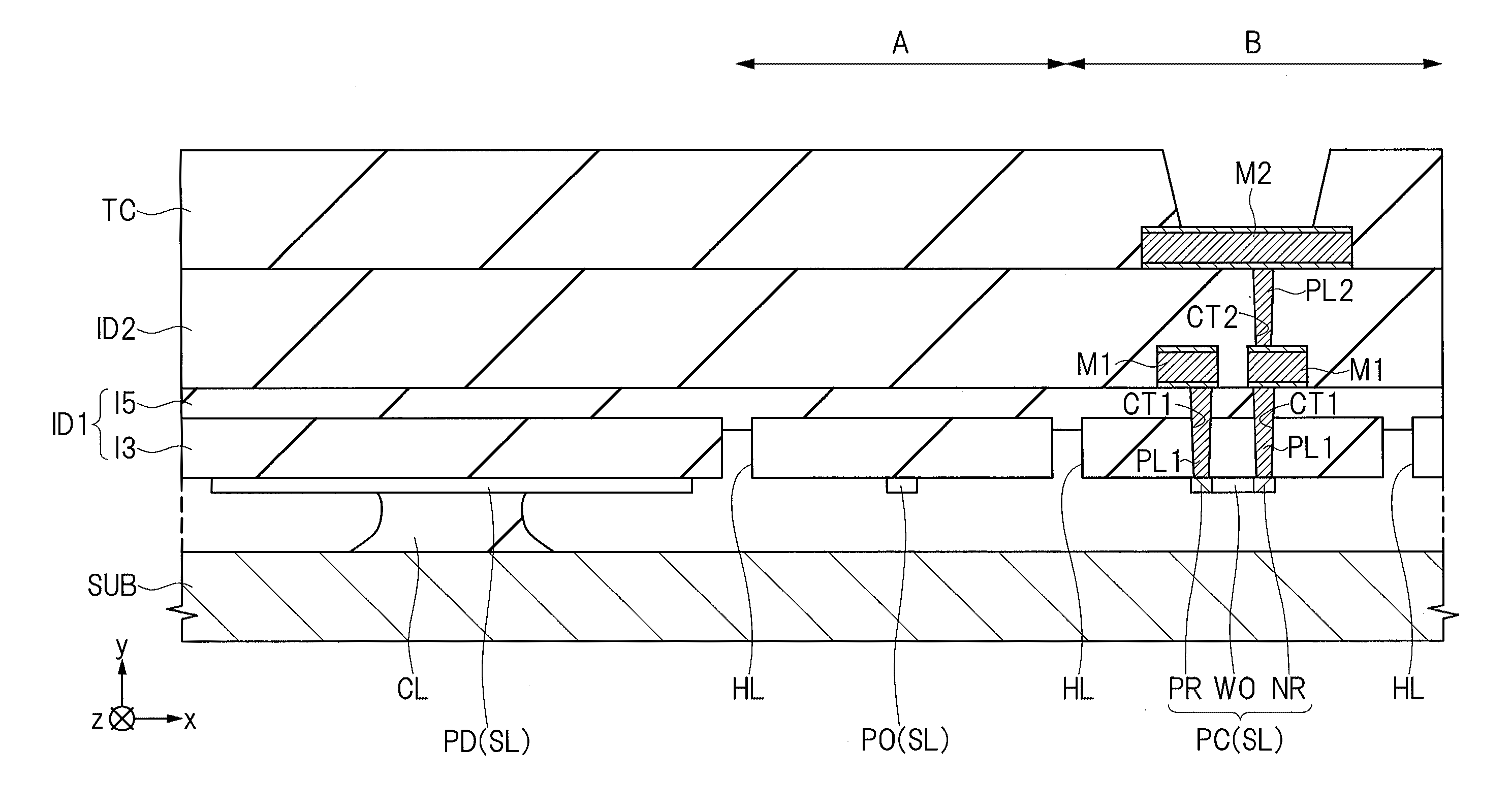
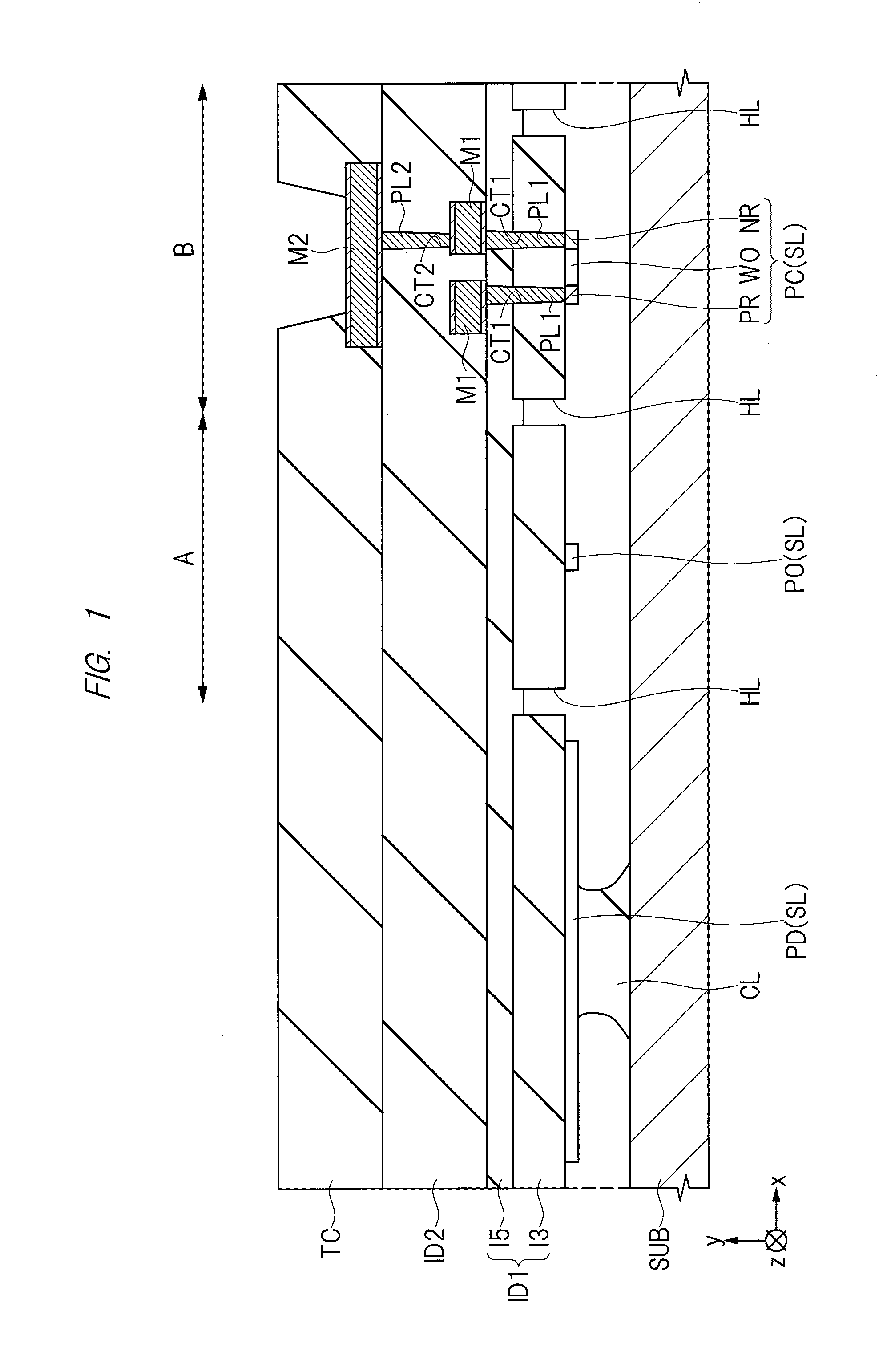
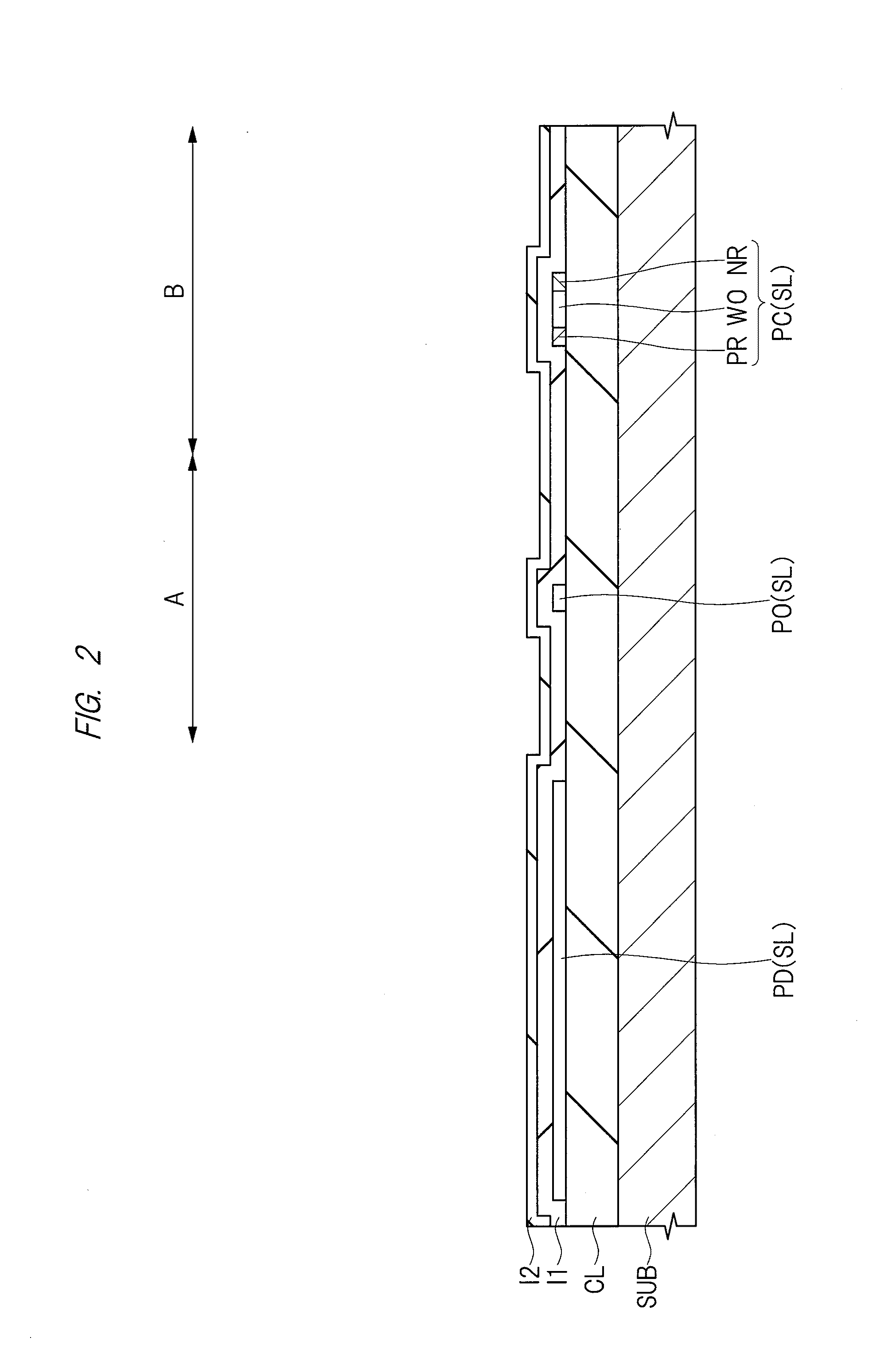
[0040]In recent years, the development of the technology to realize an optical communication module by fabricating an optical signal transmission line made of silicon (Si) and integrating various optical devices and electronic devices with using an optical circuit constituted of the optical signal transmission line as a platform, that is, the silicon photonics technology has been actively pursued.
[0041]The technology disclosed in the first embodiment is applied in particular to an optical device among various devices constituting a semiconductor device using the silicon photonics technology. For this reason, in the following description, a structure and a manufacturing method of a semiconductor device having an optical signal transmission line section and an optical modulation section integrated on an SOI substrate will be described. In addition, in the following description, an optical signal transmission line section and an optical modulation section of the optical device are illu...
second embodiment
[0098]The second embodiment is different from the first embodiment in the shape of the cavity which covers the semiconductor layer SL. Namely, three surfaces such as both side surfaces and a lower surface of each of the semiconductor layers SL constituting the optical waveguide PO and the optical modulator PC are covered with air in the first embodiment, while only both side surfaces of each of the semiconductor layers SL constituting the optical waveguide PO and the optical modulator PC are covered with air and lower surfaces thereof are covered with the insulating layer CL in the second embodiment.
[0099]Since the semiconductor device of the second embodiment is almost the same as the semiconductor device of the first embodiment described above except for the structure of the cavity and the forming method of the cavity, the difference therebetween will be mainly described below.
[0100]
[0101]A structure of the semiconductor device of the second embodiment will be described with refer...
third embodiment
[0118]The third embodiment is different from the first embodiment in the shape of the cavity which covers the semiconductor layer SL. Namely, three surfaces such as both side surfaces and a lower surface of each of the semiconductor layers SL constituting the optical waveguide PO and the optical modulator PC are covered with air in the first embodiment, while three surfaces such as both side surfaces and an upper surface (surface facing toward a side opposite to the semiconductor substrate SUB) of each of the semiconductor layers SL constituting the optical waveguide PO and the optical modulator PC are covered with air in the third embodiment.
[0119]Since the semiconductor device of the third embodiment is almost the same as the semiconductor device of the first embodiment described above except for the structure of the cavity and the forming method of the cavity, the difference therebetween will be mainly described below.
[0120]
[0121]A structure of the semiconductor device of the thi...
PUM
 Abstract
Description
Claims
Application Information