Low loss microring resonator device

a micro-ring resonator and low-loss technology, applied in the field of low-loss micro-ring resonators, can solve the problems of increasing scattering losses, reducing the minimum size of resonators, and bending become a great loss source, so as to reduce propagation losses

Inactive Publication Date: 2007-03-29
PIRELLI & C
View PDF6 Cites 11 Cited by
  • Summary
  • Abstract
  • Description
  • Claims
  • Application Information

AI Technical Summary

Benefits of technology

[0021] The present invention relates to a low loss micro-ring resonator device, and to a method to reduce the propagation losses of a resonator device, preferably for DWDM applications, configured so that its propagation losses are minimized.

Problems solved by technology

The minimum size of a resonator is limited, among others, by the bending induced losses associated with the smallest radius of curvature.
It is known that the bends become a great source of loss when the radius of curvature is less than a certain value.
In particular, as Δn increases, scattering losses also increases.
Basically, scattering losses are caused by the interaction of light with side-wall roughness of the waveguide.
Applicants have noted that this solution is feasible only for bends of few degrees and extremely localized, otherwise losses will be extremely important.
Applicants have noted that depositing the tunable cladding only over the ring core can be technologically demanding due to the limited core dimensions and that the bending losses are only partially reduced.
Applicants have pointed out that the refractive index difference between the core and the buffer is very low and it is not suitable for fabrication of small rings, i.e. rings having radius of the order of few μm, which are of interest for DWDM applications.
It is also worth noting that a buffer and upper cladding having the same refractive index is not the optimal configuration for bending losses reduction.
Additionally, in case a tunable micro-ring is desired, Applicants have noted that employment of polymeric materials in the waveguide core region—as in the article's examples—makes polymer stability a crucial issue and may affect long-term reliability of the resonator which acts as a filter.
In any case, the polymers disclosed in the article are not suitable for tuning.
On the contrary, losses are sharply increased when the cladding refractive index is increased outside this limited range.

Method used


Image

  • Low loss microring resonator device
  • Low loss microring resonator device
  • Low loss microring resonator device

Examples


example 1

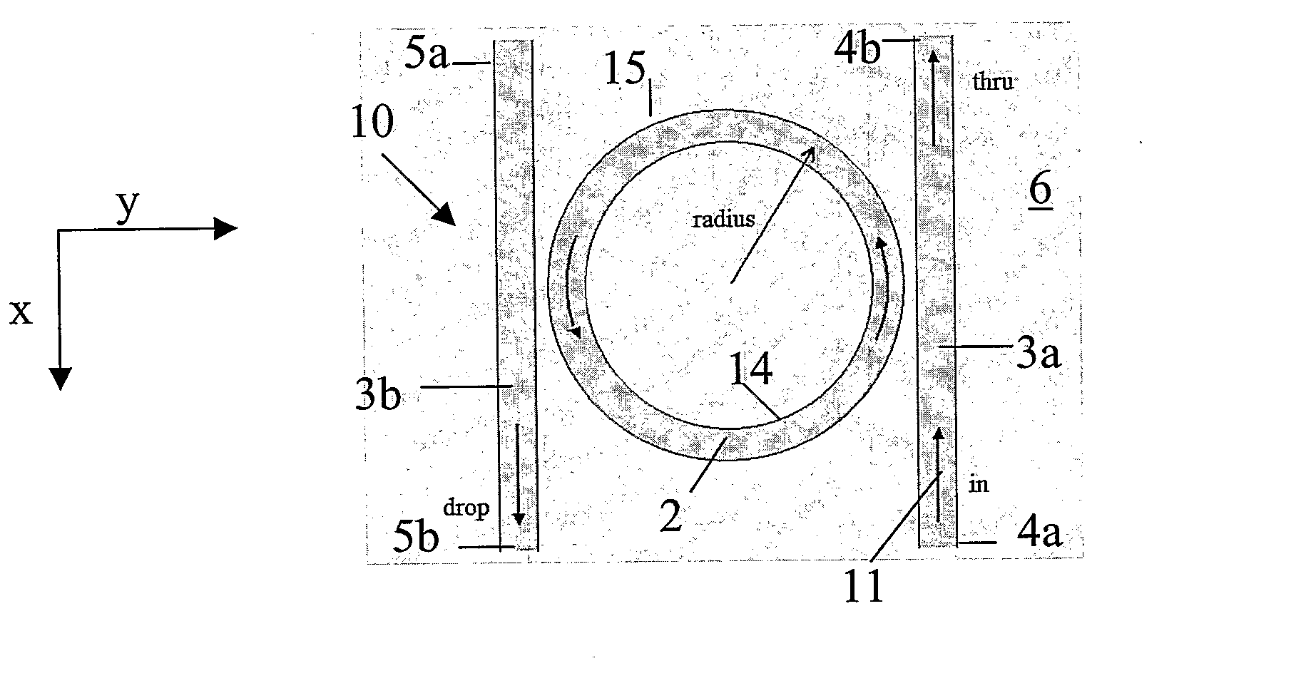
[0096] The resonator device 10 of FIG. 6 is studied. Resonator and bus waveguides 2,3a,3b lie on the same (X,Y) plane and the gap between the first or second waveguide 3a,3b and the resonator 2 is comprised between 100 and 150 nm. The substrate 6 is SiO2 having refractive index nr=1.45, while the resonator waveguide 2 and the bus waveguides 3a, 3b are realized in Si-rich Si3N4 having nb=2.2. The lateral cladding 21 is air (nlc=1) and the upper cladding 20 is a Sylgard™ 184 (nuc=1.4005 at room temperature) film of a thickness h of 3 μm. Refractive indices are taken at a wavelength of 1550 nm. The cross-section of the bus and resonant waveguides is a 1000×300 nm rectangle with 100 nm over-etch. The resonator waveguide 2 is a ring having radius of 7 μm.

[0097] Applicants have found that the round trip total losses α of this device 10 are equal to α=0.07 dB / round trip. If the Sylgard covers the entire device, i.e. upper and lateral cladding are made of Sylgard, the losses become α=0.55 ...

example 2

[0098] The device 10 is identical to the device of Example 1 except for the waveguides cross-section, which is in this case a rectangle of 1200×250 nm and has 200 nm over-etch. The losses are equal to α=0.1 dB / round trip or, equivalently, α=22.7 dB / cm. In FIGS. 13 and 14, the graphs of FIGS. 3 and 4 are reproduced and a circle is added in each graph showing the bending and scattering losses, respectively, of the studied device 10 of this example. From the figures, it is clear that the device 10 of the invention, with respect to the device 50 in which both upper and lateral cladding are air, but all other construction characteristics being the same, has much lower bending losses, while the scattering losses are almost unaffected.

example 3

[0099] The device 10, in which bus and resonator waveguides all lie on the same plane, has the following characteristics: [0100] substrate 6: SiO2; nr=1.45, [0101] resonant waveguide 2, bus waveguides 3a, 3b: Si-rich Si3N4; nb=2.2, [0102] lateral cladding 21: air; nlc=1 [0103] cross-section of all waveguides: 1000×300 nm rectangle with 100 nm over-etch

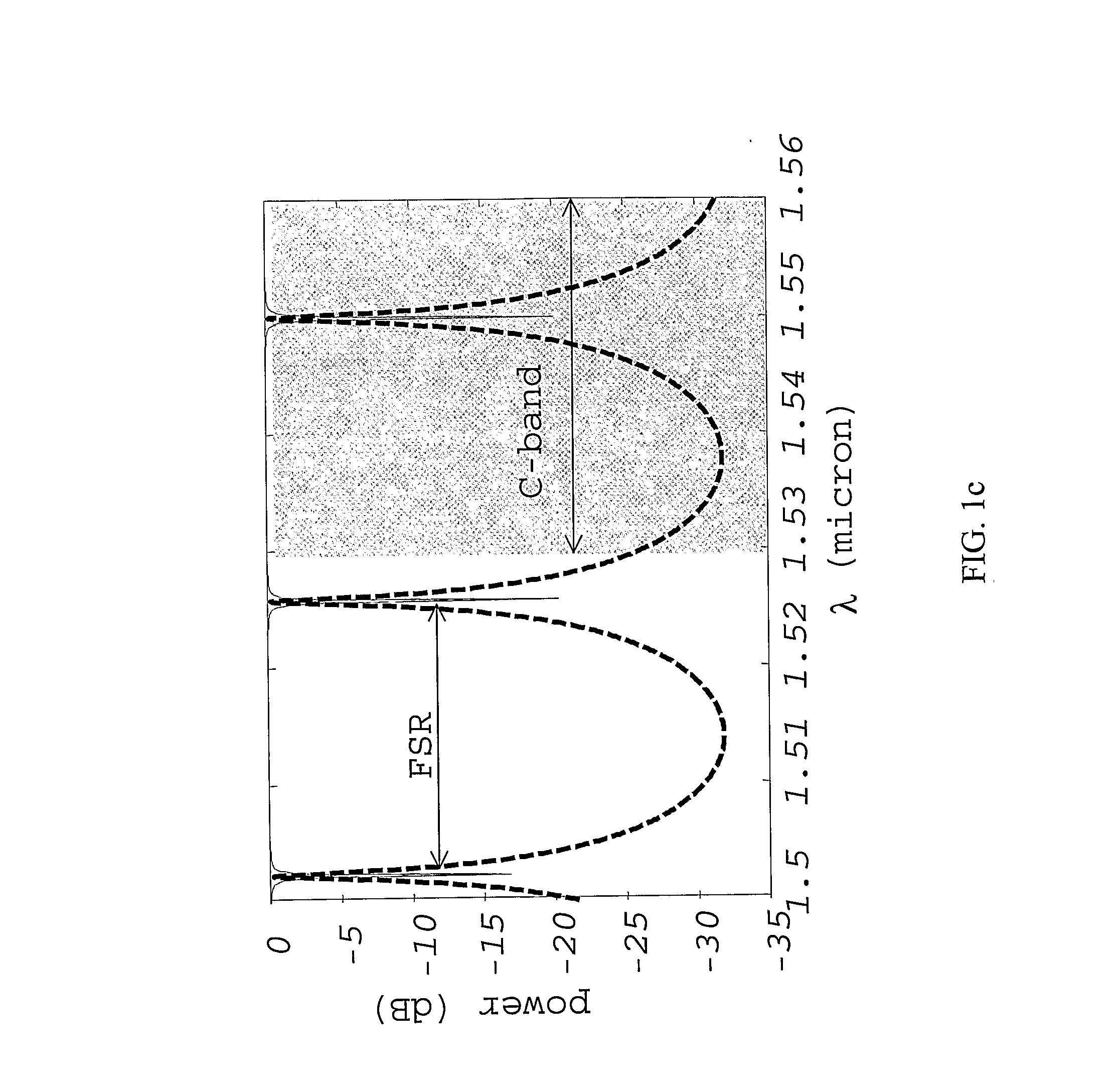
[0104] The propagation losses of this device have been computed for different resonator waveguide radii and different refractive indices of the upper cladding 20. The results are plotted in FIG. 8: the round-trip losses as a function of nuc are shown for a ring radius of 5 (FSR=36 nm), 6 (FSR=30 nm), 7 (FSR=26 nm) and 8 μm (FSR=23 nm).

[0105] For the desired applications, the maximum admissible total loss is equal to 0.1 dB / round trip (equal to 22.7 dB / cm). Therefore from FIG. 8, the useful range of the refractive index of an applicable upper cladding 20 can be derived. For example, for a ring having R2=7 μm, the useful nuc range is 1...


PUM

PropertyMeasurementUnit
wavelengthsaaaaaaaaaa
radiusaaaaaaaaaa
radiusaaaaaaaaaa

Abstract

A low loss micro-ring resonator device which has a closed-loop resonator waveguide having a first refractive index, the resonator waveguide defining an inner and an outer region by an outer curved edge of the waveguide. The resonator waveguide is arranged on a substrate having a second refractive index, the refractive index difference between the first refractive index and the second refractive index is greater than 0.3. The device also has an upper cladding covering the inner region of the resonator waveguide having a third refractive index and a lateral cladding in contact with the outer curved edge and extending in the outer region, the lateral cladding having a fourth refractive index, the fourth refractive index being lower than the third refractive index. A method for reducing propagation losses of a resonator device is also described.

Description

TECHNICAL FIELD [0001] The present invention relates to a low loss micro-ring resonator device, in which propagation losses are minimized for a given resonator device configuration. Additionally, the invention is also relative to a method to reduce propagation losses in a resonator device. TECHNOLOGICAL BACKGROUND [0002] Micro-resonators have shown considerable versatility over the last decade as candidates for wavelength filtering, routing, switching, modulation, dispersion compensators, laser and multiplexing / demultiplexing applications. Their size has progressively decreased and therefore they have attracted considerable attention for their potential use in integrated optical devices making all-optical signal processing a closer possibility. [0003] A small resonator size is also extremely important in dense wavelength division multiplexed (DWDM) systems, which require optical filters characterized by high selectivity and large FSR (Free Spectral Range). [0004] A resonator consist...

Claims


Application Information

Patent Timeline
Patent Type & Authority Applications(United States)
IPC IPC(8): G02B6/10G02B6/12G02B6/34G02F1/01G02F1/065
CPCG02B6/12007G02B6/29343G02B6/29352G02B6/29383G02B6/29389G02F2203/15G02B2006/12119G02F1/011G02F1/0118G02F1/065G02F2203/055G02B6/29395
Inventor FACCIO, DANIELE FRANCO ANGELOROMAGNOLI, MARCO
Owner PIRELLI & C
Why Eureka
Try Eureka