Spst Switch, Spdt Switch and Mpmt Switch

a single-pole, multi-pole technology, applied in the direction of electronic switching, pulse technique, electrical equipment, etc., can solve the problems of reducing the isolation of the high-frequency signal from the input terminal, propagating etc., to prevent the reduction of the isolation reduce the propagation loss of the high-frequency signal, and the effect of high power

Inactive Publication Date: 2008-10-02
MITSUBISHI ELECTRIC CORP
View PDF4 Cites 11 Cited by
  • Summary
  • Abstract
  • Description
  • Claims
  • Application Information

AI Technical Summary

Benefits of technology

[0014]According to the present invention, an advantage is obtained of being able to achieve high withstanding power, and to reduce the propagation loss of the high frequency signal from the input terminal to the output terminal, and to prevent reduction in the isolation of the high frequency signal from the input terminal to the output terminal.

Problems solved by technology

Accordingly, when the FET 2a and FET 2b are brought into the OFF state, the propagation loss of the high frequency signal propagating from the input terminal 1a to the output terminal 1b increases, which presents a problem of reducing the isolation of the high frequency signal from the input terminal 1a to the output terminal 1c.
Although the conventional technique is described by way of example of the SPDT switch, an SPST switch or MPMT switch has the same problem.

Method used


Image

  • Spst Switch, Spdt Switch and Mpmt Switch
  • Spst Switch, Spdt Switch and Mpmt Switch
  • Spst Switch, Spdt Switch and Mpmt Switch

Examples


embodiment 1

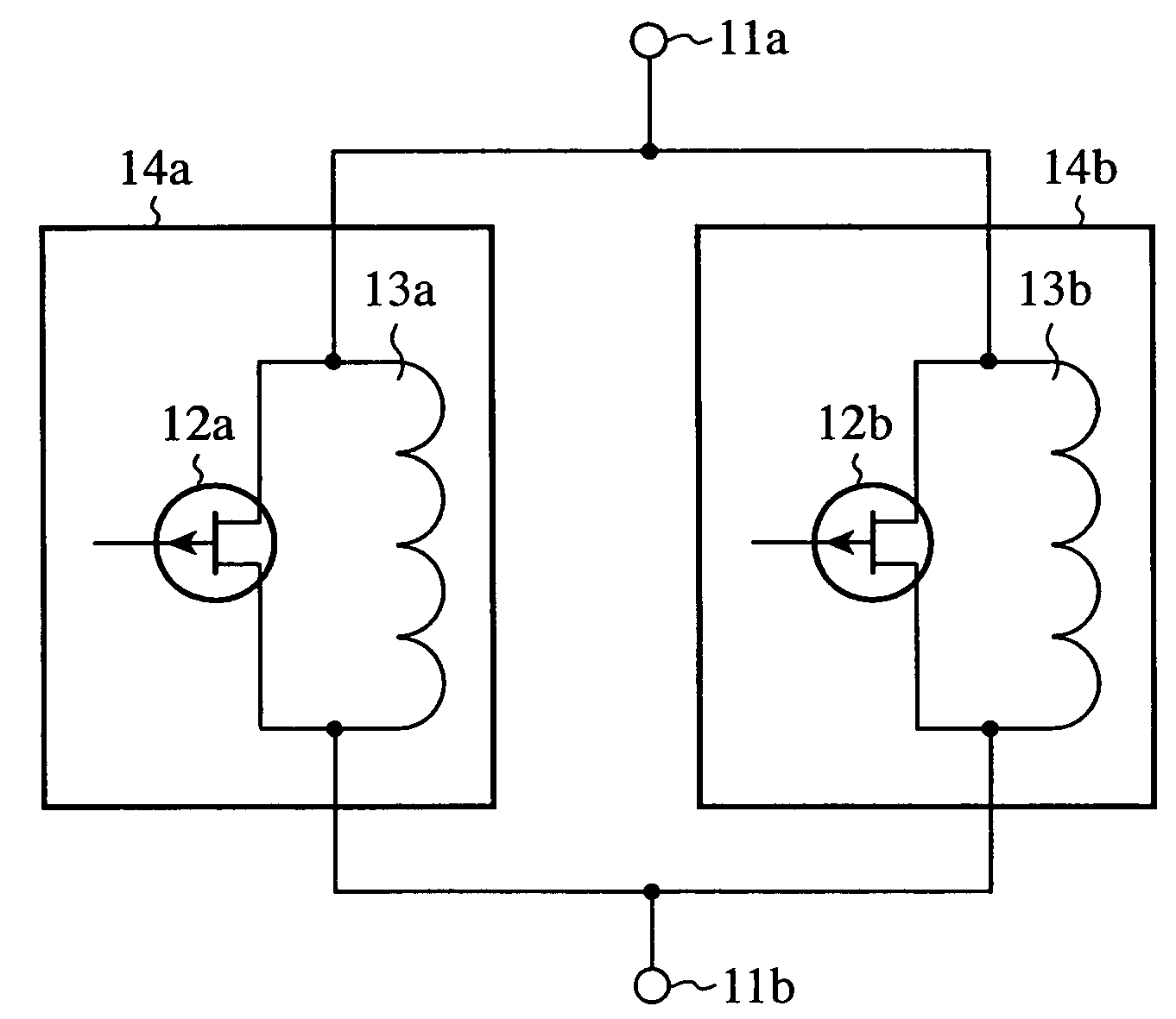
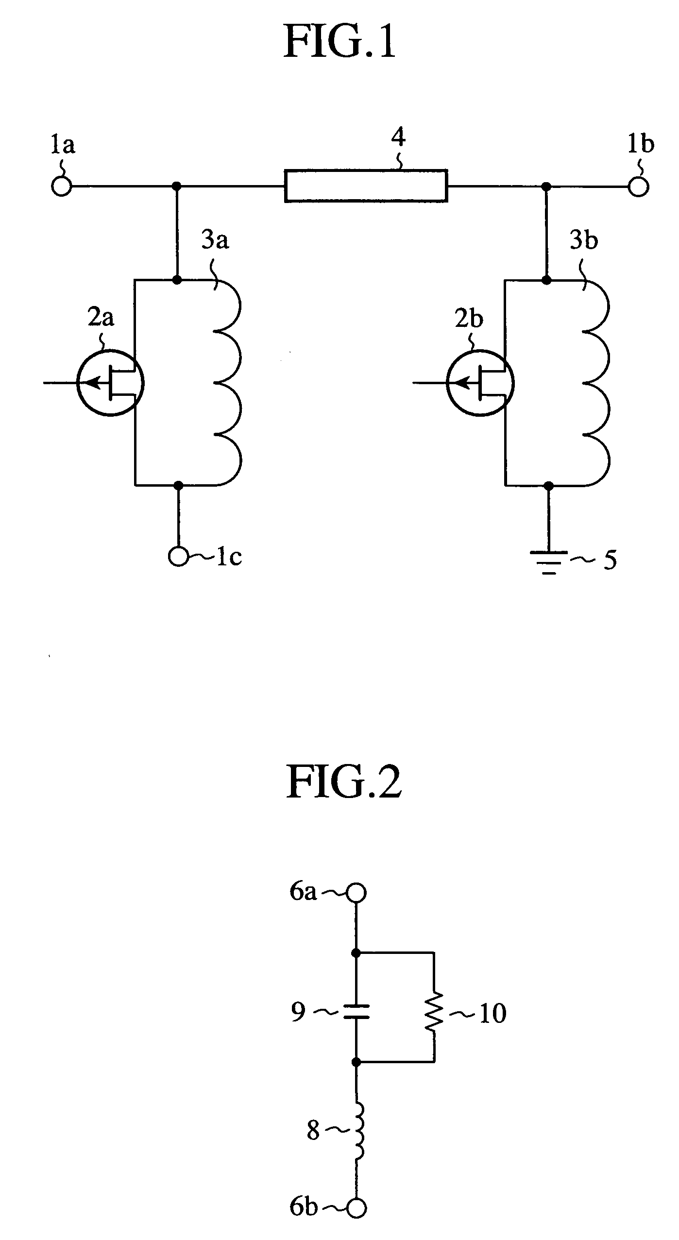
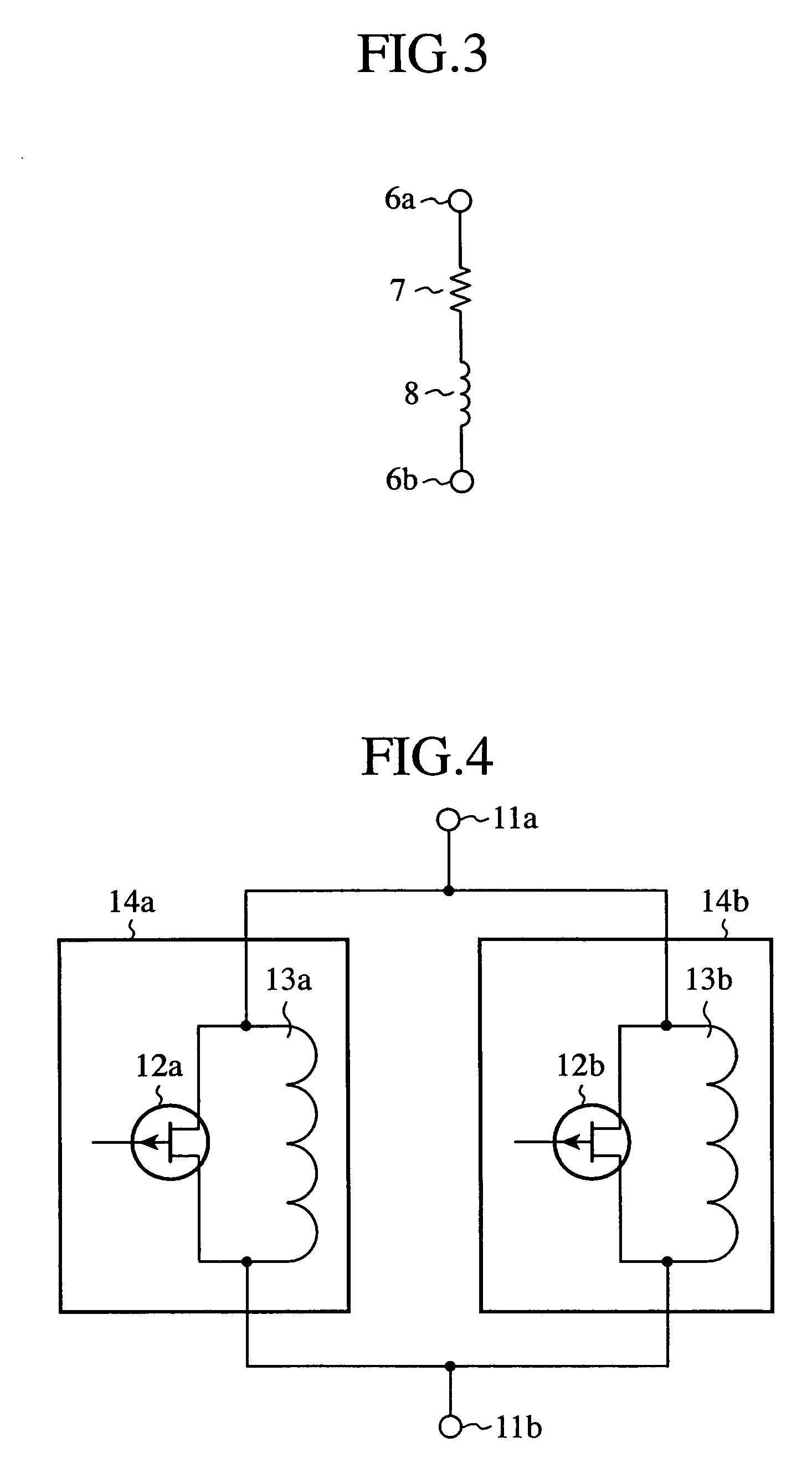
[0042]FIG. 4 is a circuit diagram showing a configuration of an SPST switch of an embodiment 1 in accordance with the present invention. The SPST switch shown in FIG. 4 has an input terminal 11a, output terminal 11b, FET (field-effect transistor) 12a, FET 12b, inductor 13a and inductor 13b. The parallel connection of the FET 12a and inductor 13a constitutes a first FET switch 14a, and the parallel connection of the FET 12b and inductor 13b constitutes a first FET switch 14b. The FET switches 14a and 14b have their first terminals connected to the input terminal 11a, and their second terminals connected to the output terminal 11b. Thus, the first FET switch 14a is connected in parallel with the first FET switch 14b in the present embodiment 1.

[0043]Connecting the two FETs 12a and 12b in parallel can halve their individual gate width to achieve the same withstanding power. Halving the individual gate width can make the reactance components of the parasitic inductors of the FETs 12a an...

embodiment 2

[0054]FIG. 7 is a circuit diagram showing a configuration of an SPST switch of an embodiment 2 in accordance with the present invention. As the SPST switch of the embodiment 1 shown in FIG. 4, the SPST switch shown in FIG. 7 has an input terminal 11a, output terminal 11b, FET 12a, FET 12b, inductor 13a and inductor 13b. The parallel connection of the FET 12a and inductor 13a constitutes a first FET switch 14a, and the parallel connection of the FET 12b and inductor 13b constitutes a first FET switch 14b. The embodiment 2, however, differs from the embodiment 1 in that the input terminal 11a and the output terminal 11b are connected directly, and in that the first FET switch 14a and first FET switch 14b have their first terminals connected to the input terminal 11a and output terminal 11b, and their second terminals connected to the ground 19. Thus, in the present embodiment 2, the first FET switch 14a is connected in parallel with the first FET switch 14b.

[0055]Connecting the two F...

embodiment 3

[0066]FIG. 10 is a circuit diagram showing a configuration of an SPST switch of an embodiment 3 in accordance with the present invention. The SPST switch shown in FIG. 10 has an input terminal 11a, output terminal 11b, FET 20, capacitor 21 and inductor 22. A second FET switch 14, which consists of a series connection of the FET 20 and capacitor 21, and the inductor 22 connected in parallel with the series connection, has its first terminal connected to the input terminal 11a, and has its second terminal connected to the output terminal 11b.

[0067]Here, the drain of the FET 20 can be connected to the input terminal 11a or capacitor 21, and the source of the FET 20 can be connected to the capacitor 21 or input terminal 11a.

[0068]Next the operation will be described.

[0069]In FIG. 10, the FET 20 operates as a switch for switching between the ON state and OFF state by the voltage applied to the gate.

[0070]FIG. 11 is an equivalent circuit diagram when the FET 20 in FIG. 10 is brought int...


PUM


Abstract

A single pole single throw switch for controlling propagation of a high frequency signal between an input terminal (11a) and an output terminal (11b). First FET switches (14a, 14b) in which drains and sources of FETs (12a, 12b) are connected in parallel with inductors (13a, 13b) are connected in parallel. Each FET (12a, 12b) is switched between on state and off state by a voltage being applied to the gate thereof. At the frequency of the high frequency signal, each inductor (13a, 13b) connected with off capacitor of each FET (12a, 12b) resonates in parallel.

Description

TECHNICAL FIELD[0001]The present invention relates to a single-pole single-throw (SPST) switch, a single-pole double-throw (SPDT) switch and a multiple-pole multiple-throw (MPMT) switch for controlling propagation of a high frequency signal.BACKGROUND ART[0002]FIG. 1 is a circuit diagram showing a conventional SPDT switch shown in “High-power microwave transmit-receive switch with series and shunt GaAs FETs”, IEICE Trans. ELECTRON, February 1992.[0003]The SPDT switch as shown in FIG. 1 has an input terminal 1a, output terminal 1b, output terminal 1c, FET (field-effect transistor) 2a, FET 2b, inductor 3a, inductor 3b, line 4 and ground 5. The FET 2a has its drain connected to the input terminal 1a, and its source connected to the output terminal 1c. The inductor 3a has its first terminal connected to the input terminal 1a, and its second terminal connected to the output terminal 1c. The line 4 has its first terminal connected to the input terminal 1a, and its second terminal connecte...

Claims


Application Information

Patent Timeline
Patent Type & Authority Applications(United States)
IPC IPC(8): H01P1/15H03K17/00H03K17/06
CPCH01P1/15
Inventor HANGAI, MASATAKEHIEDA, MORISHIGEMIYAZAKI, MORIYASU
Owner MITSUBISHI ELECTRIC CORP
Why Eureka
Try Eureka