Method and device for controlling bias of optical modulator

a technology of optical modulator and bias, applied in the direction of optics, electrical apparatus, instruments, etc., can solve the problems of inability to correct stationary optical communication or optical measurement, complex configuration related to the control of dc bias of optical modulator, and change in output characteristics of light with time, so as to reduce the burden on the circuit for extracting the change of light intensity corresponding to each low frequency electrical signal. , to achieve the effect of accurate understanding input/output characteristics, reducing the burden

Inactive Publication Date: 2007-01-25
SUMITOMO OSAKA CEMENT CO LTD
View PDF5 Cites 49 Cited by
  • Summary
  • Abstract
  • Description
  • Claims
  • Application Information

AI Technical Summary

Benefits of technology

[0051] In accordance with the invention related to claim 1, by applying the specific low frequency electrical signal into each optical modulating section and detecting the change of light intensity corresponding thereto, it becomes possible to easily understand the state of the drift phenomenon of each optical modulating section. Further, control of the DC bias of each optical modulating section becomes possible even while using the optical modulator without complicating the optical modulator and bias controlling circuit too much.
[0063] In accordance with the invention related to claim 14, the plurality of optical detectors are placed corresponding to the plurality of optical modulating sections to decrease the number of optical modulating sections assigned to one optical detector. Thus, it is possible to select the optical detector in accordance with the frequency of the low frequency electrical signal. This increases the range of said frequency choices while the burden on the circuit for extracting the change of light intensity corresponding to each low frequency electrical signal can be reduced.

Problems solved by technology

However, such optical modulator is known for causing a so-called drift phenomenon that the output characteristics of light change with time due to the amount of the applied DC bias for drive control or due to the temperature change of its operating environment.
As stated above, configuration related to control of DC bias of optical modulator gets complicated in accordance with the increasing optical modulating sections.
Further, there occurs the problem that correction is not possible in stationary optical communication or optical measurement because, when the input / output characteristics of a specific optical modulating section are measured, the other optical modulating sections are made not to operate.

Method used


Image

  • Method and device for controlling bias of optical modulator
  • Method and device for controlling bias of optical modulator
  • Method and device for controlling bias of optical modulator

Examples


Embodiment Construction

[0072] In the following, the preferred embodiments of the present invention are explained in detail.

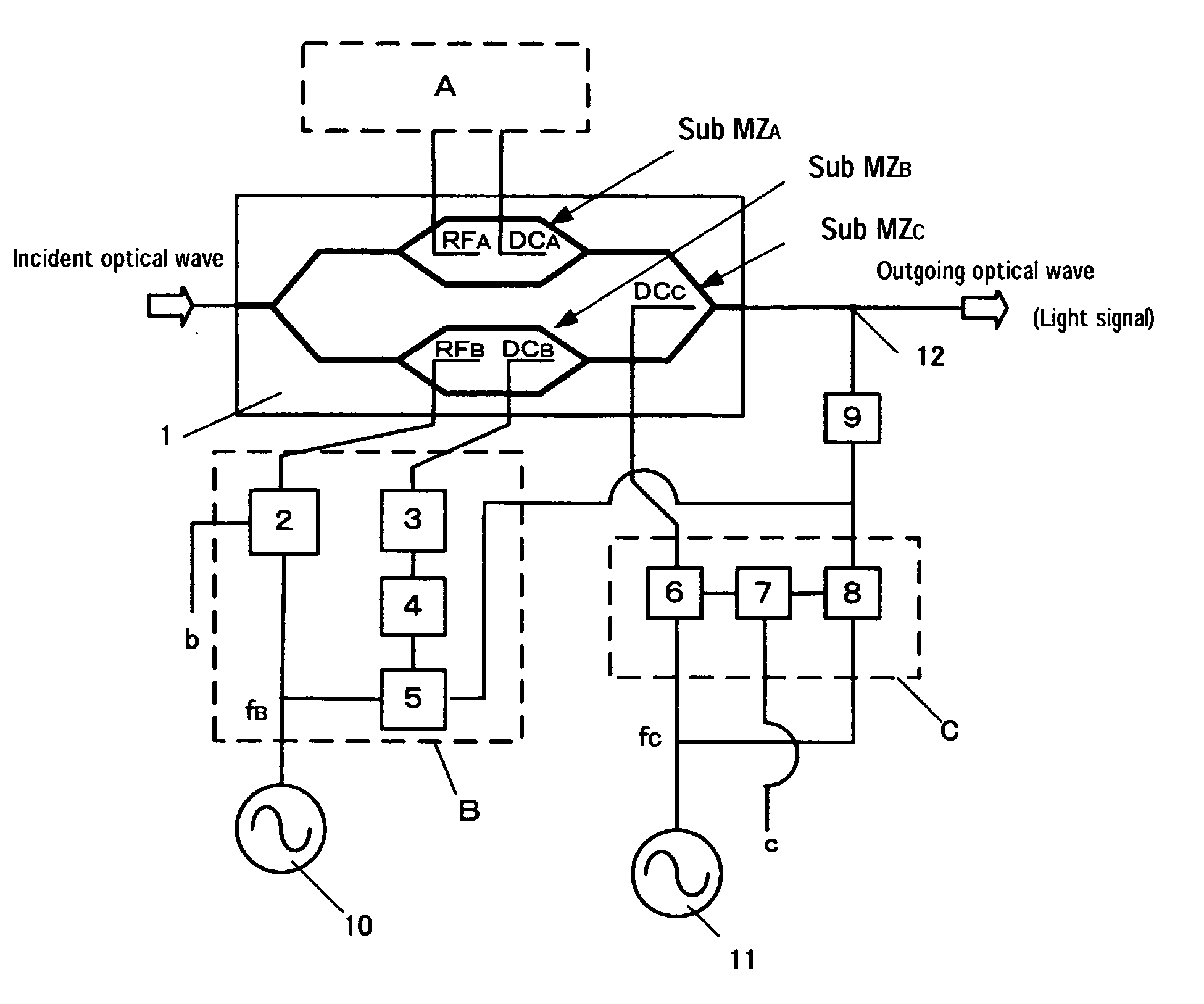
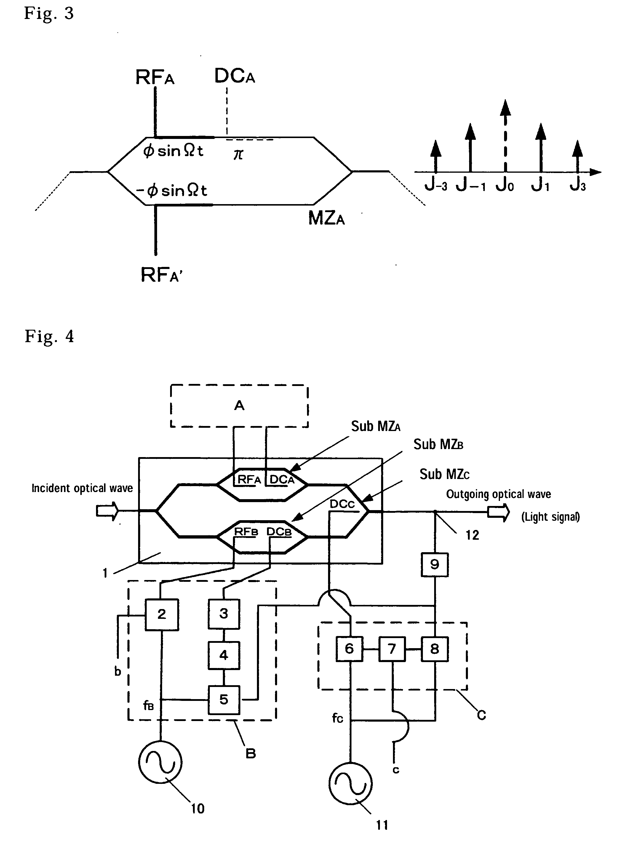
[0073]FIG. 4 is a schematic diagram of one embodiment of the device for controlling the bias of the optical modulator according to the present invention.

[0074] An optical modulator 1 is the nesting optical intensity modulator explained in FIG. 1. An optical wave such as a laser enters optical modulator 1, receives predetermined modulation while propagating through said optical modulator 1, and exits from optical modulator 1 as a light signal.

[0075] Although the nesting optical intensity modulator is explained as the example in the following, the present invention is not limited to this but it is possible to apply the present invention to an optical modulator comprised of a plurality of optical modulating sections (sections having the function of intensity modulation or phase modulation) combined together.

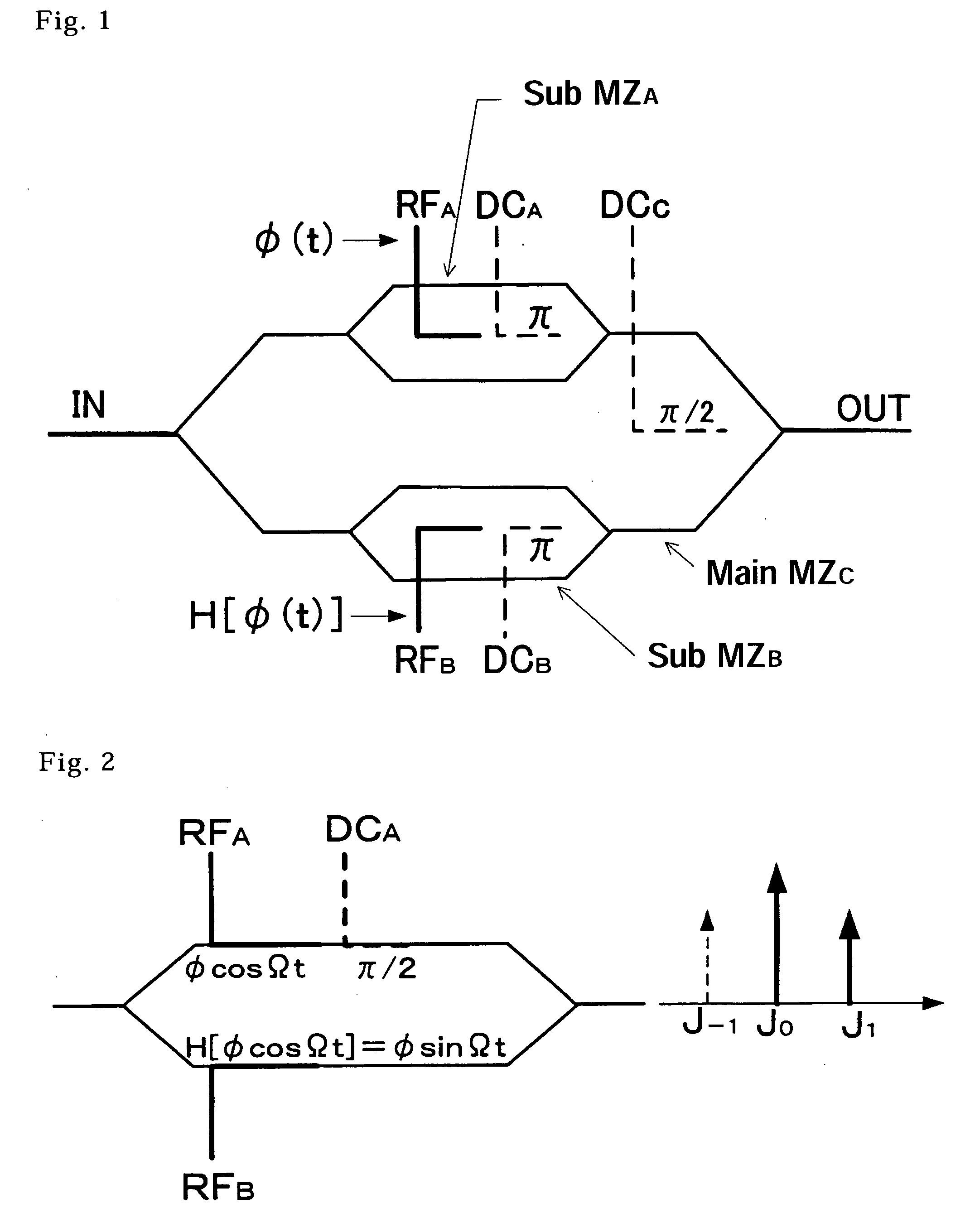
[0076] The sub MZ type optical waveguides MZA, MZB and main MZ type optical w...


PUM

PropertyMeasurementUnit
frequencyaaaaaaaaaa
light intensityaaaaaaaaaa
specific frequencyaaaaaaaaaa

Abstract

A method and device for adequately controlling the DC bias of each of the optical modulating sections of an optical modulator even while the optical modulator is operating in normal mode and even with a simple structure. An optical modulator bias controller (B) for controlling the DC bias of each optical modulating section of an optical modulator (1) is characterized by comprising DC bias application means (3) for applying a DC bias to each of the optical modulating sections, a low-frequency signal superimposing circuit (2) for superimposing a low-frequency signal fB with a specific frequency on a modulating signal b applied to each optical modulating section, optical sensing means (9) for sensing a change of the intensity of the light wave passing through the combining section, and bias control means (4) for extracting the change of the intensity of light corresponding to the low-frequency signal from the optical sensing means and controlling the DC bias application means according to the extracted change of the intensity of light.

Description

BACKGROUND OF THE INVENTION [0001] (1) Field of the Invention [0002] The present invention relates to a method and device for controlling bias of optical modulator, and more particularly to a method and device for controlling bias of optical modulator for adequately controlling the DC bias of each of a plurality of optical modulating sections of an optical modulator comprising the plurality of optical modulating sections therein. [0003] (2) Related Art Statement [0004] Optical modulator is frequently used as an electrical-optical conversion device in the field of optical communication or optical measurement. [0005] An optical intensity modulator comprising a substrate with an electro-optic effect such as LiNbO3 is cited as an example of the optical modulator. However, such optical modulator is known for causing a so-called drift phenomenon that the output characteristics of light change with time due to the amount of the applied DC bias for drive control or due to the temperature ch...

Claims


Application Information

Patent Timeline
Patent Type & Authority Applications(United States)
IPC IPC(8): H04B10/04G02F1/01G02F1/03G02F1/035G02F1/225
CPCG02F1/0123G02F1/0327G02F2201/58G02F1/225G02F1/035
Inventor HASHIMOTO, YOSHIHIROICHIKAWA, JUNICHIROHIGUMA, KAORUFUJITA, TAKAHISA
Owner SUMITOMO OSAKA CEMENT CO LTD
Why Eureka
Try Eureka