Semiconductor failure analysis apparatus, failure analysis method, and failure analysis program

a technology of failure analysis and failure parts, applied in semiconductor/solid-state device testing/measurement, instruments, image enhancement, etc., can solve the problems of difficult to perform the analysis of failure parts by means of the aforementioned inspection apparatus, and achieve high possibility of failure, and efficient failure analysis

Inactive Publication Date: 2007-01-25
HAMAMATSU PHOTONICS KK
View PDF22 Cites 9 Cited by
  • Summary
  • Abstract
  • Description
  • Claims
  • Application Information

AI Technical Summary

Benefits of technology

[0010] The above-described semiconductor failure analysis apparatus, failure analysis method, and failure analysis program are arranged to acquire the failure observed image such as an emission image or OBIRCH image acquired by conducting an inspection of the semiconductor device as an analysis object, and necessary information about the layout of the semiconductor device. Then the analysis region is set in correspondence to the reaction information (e.g., information about a reaction part) in the failure observed image, and a net passing the analysis region is extracted out of the nets constituting the semiconductor device, thereby performing the analysis of the failure of the semiconductor device. This configuration permits us to estimate a net with a high possibility of failure in the semiconductor device by suitably setting the analysis region and extracting the net passing the analysis region. Therefore, it becomes feasible to securely and efficiently perform the analysis of the failure of the semiconductor device with the use of the failure observed image.
[0011] Since the semiconductor failure analysis apparatus, failure analysis method, and failure analysis program of the present invention are arranged to set the analysis region in correspondence to the reaction information in the failure observed image and to extract a net passing the analysis region out of the nets in the layout of the semiconductor device, they permit us to estimate a net with a high possibility of failure in the semiconductor device by suitably setting the analysis region and extracting a net passing the analysis region. Therefore, it becomes feasible to securely and efficiently perform the analysis of the failure of the semiconductor device with the use of the failure observed image.

Problems solved by technology

In recent years, semiconductor devices as analysis objects in the semiconductor failure analysis have been miniaturized and integrated more and more, and it has become difficult to perform the analysis of failure part by means of the aforementioned inspection apparatus.

Method used


Image

  • Semiconductor failure analysis apparatus, failure analysis method, and failure analysis program
  • Semiconductor failure analysis apparatus, failure analysis method, and failure analysis program
  • Semiconductor failure analysis apparatus, failure analysis method, and failure analysis program

Examples


Embodiment Construction

[0024] Preferred embodiments of the semiconductor failure analysis apparatus, failure analysis method, and failure analysis program according to the present invention will be described below in detail with reference to the drawings. In the description of the drawings the same elements will be denoted by the same reference symbols, without redundant description. It is also noted that dimensional ratios in the drawings do not always agree with those in the description.

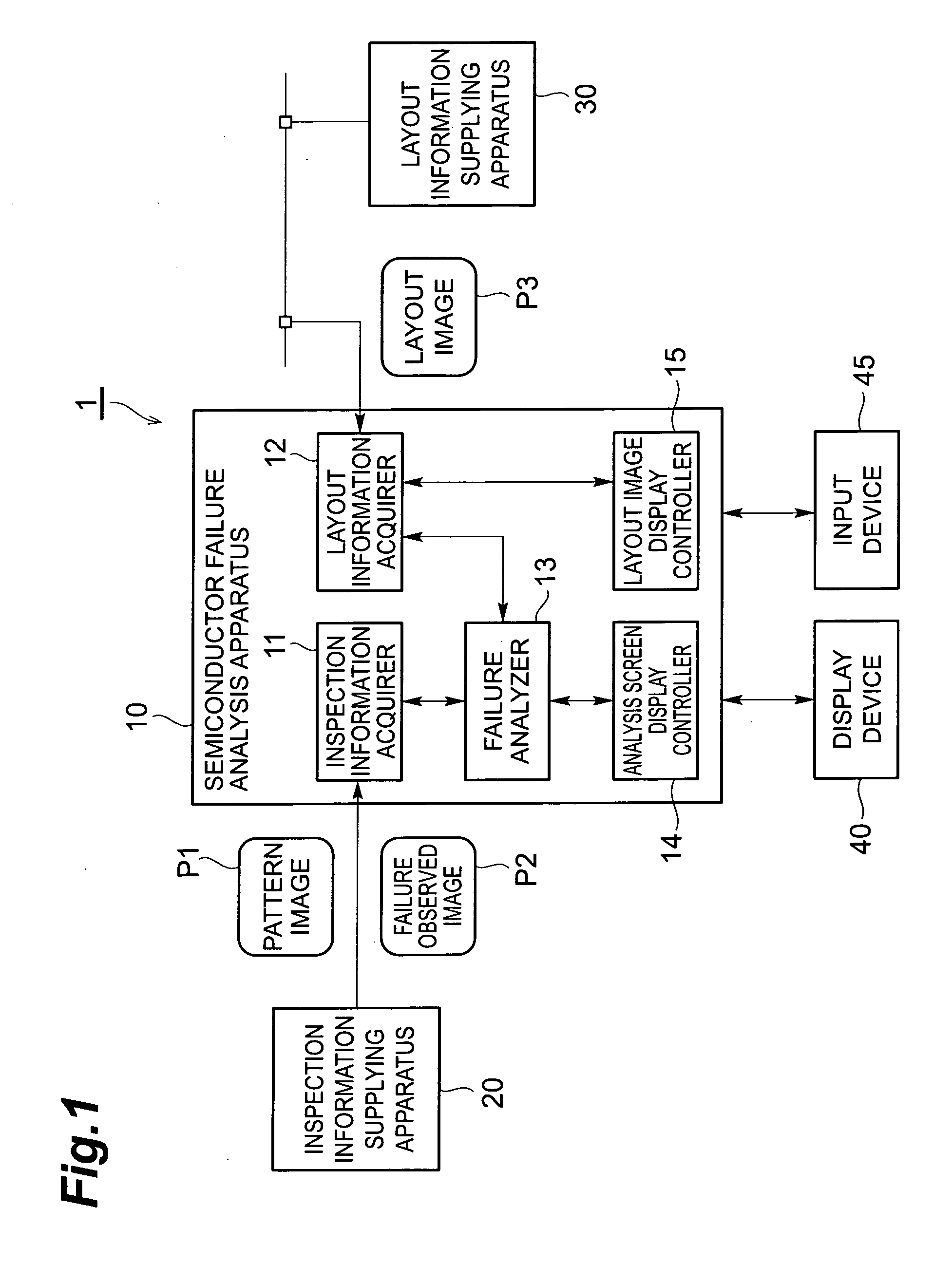
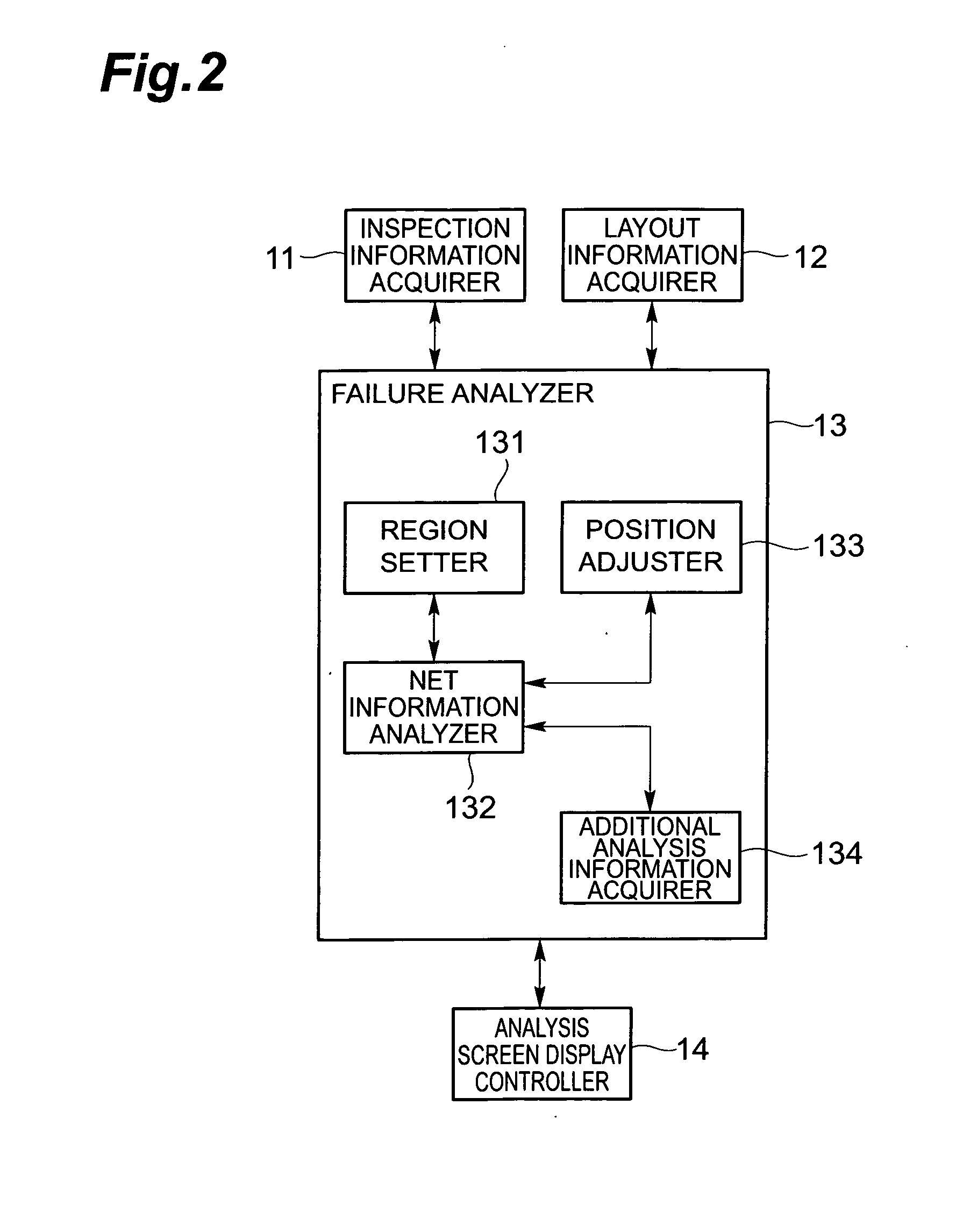
[0025]FIG. 1 is a block diagram schematically showing a configuration of an embodiment of the failure analysis system incorporating the semiconductor failure analysis apparatus according to the present invention. The present failure analysis system 1 is a system an analysis object of which is a semiconductor device and which is for carrying out an analysis of a failure with the use of an observed image thereof, and the system comprises a semiconductor failure analysis apparatus 10, an inspection information supplying ap...


PUM


Abstract

A failure analysis apparatus 10 is composed of an inspection information acquirer 11 for acquiring a failure observed image P2 of a semiconductor device, a layout information acquirer 12 for acquiring layout information, a failure analyzer 13 for analyzing a failure of the semiconductor device, and an analysis screen display controller 14 for letting a display device 40 display information about a result of the analysis. The failure analyzer 13 sets an analysis region with reference to the failure observed image P2, and extracts a net passing the analysis region, from a plurality of nets included in a layout of the semiconductor device. This substantializes a semiconductor failure analysis apparatus, analysis method, and analysis program capable of securely and efficiently performing the analysis of the failure of the semiconductor device.

Description

BACKGROUND OF THE INVENTION [0001] 1. Field of the Invention [0002] The present invention relates to a semiconductor failure analysis apparatus, failure analysis method, and failure analysis program for analyzing a failure of a semiconductor device. [0003] 2. Related Background Art [0004] The conventionally available semiconductor inspection apparatus for acquiring an observed image for analysis of failure of a semiconductor device include emission microscopes, OBIRCH apparatus, time-resolved emission microscopes, and so on. These inspection apparatus are able to analyze such a failure as a broken part in a semiconductor device by use of an emission image or OBIRCH image acquired as a failure observed image (e.g., reference is made to Patent Document 1: Japanese Patent Application Laid-Open No. 2003-86689 and to Patent Document 2: Japanese Patent Application Laid-Open No. 2003-303746). SUMMARY OF THE INVENTION [0005] In recent years, semiconductor devices as analysis objects in the ...

Claims


Application Information

Patent Timeline
Patent Type & Authority Applications(United States)
IPC IPC(8): H01L21/66
CPCG01N21/956G06T2207/30148G06T7/001G01R31/302H01L22/00
Inventor MAJIMA, TOSHIYUKISHIMASE, AKIRATERADA, HIROTOSHIHOTTA, KAZUHIROTAKEDA, MASAHIRO
Owner HAMAMATSU PHOTONICS KK
Why Eureka
Try Eureka