Processing method and grinding apparatus of wafer

a processing method and wafer technology, applied in the field of wafer processing methods, can solve the problems of difficult to handle or carry wafers after grinding, difficult to handle or carry wafers, and difficult to handle wafers, etc., and achieve the effects of easy removal, reduced thickness of device regions, and easy handling

Active Publication Date: 2007-01-25
DISCO CORP
View PDF9 Cites 24 Cited by
  • Summary
  • Abstract
  • Description
  • Claims
  • Application Information

AI Technical Summary

Benefits of technology

[0014] According to the processing method of the wafer of the invention, since the region corresponding to the device region in the back of the wafer is ground to form the concave portion so that the ring-like reinforcement portion is formed in the peripheral side of the concave portion, even if thickness of the device region is extremely reduced, the wafer is in a condition that the device region is reinforced from the peripheral side by the ring-like reinforcement portion. Accordingly, the wafer after forming the concave portion can be easily removed from the grinding apparatus, and the wafer is easily handled in a subsequent step and wafer carrying-between respective steps. Furthermore, since the whole back is ground to form the wafer in a predetermined thickness before forming the concave portion, time required for forming the concave portion in the predetermined thickness is short, and consequently reduction in productivity can be avoided.
[0015] When the grindstone is contacted to the rotation center of the wafer such that the outermost circumference of the rotational orbit of the grindstone corresponds to the inner circumference of the ring-like reinforcement portion to be formed, the ring-like reinforcement portion can be efficiently formed.
[0016] When the film formation process for forming the film on the back of the wafer after the concave-grinding process is performed, the wafer is easily handled in the film formation process and before and after the process.
[0017] According to the grinding apparatus of the invention, since the chuck table that rotatably and movably holding the wafer, whole-back grinding unit of grinding the whole back of the wafer, and device-region corresponding region grinding unit of grinding the region corresponding to the device region in the back are provided, the chuck table can be moved after the whole surface has been ground by the whole-back grinding unit so that the device-region corresponding region is ground by the device-region corresponding region grinding unit. Accordingly, two stages of grinding can be continuously performed by one grinding apparatus, and consequently grinding is efficiently performed.
[0018] Moreover, when the grindstone configuring the device-region corresponding region-grinding unit is formed such that the grindstone is contacted to the rotation center of the wafer during grinding, and the outermost circumference of the rotational orbit corresponds to the inner circumference of the ring-like reinforcement portion, the ring-like reinforcement portion can be efficiently formed.

Problems solved by technology

However, there is a difficulty that such a wafer formed thin by grinding loses stiffness and accordingly the wafer is hard to be handled or carried after grinding.
For example, when a wafer after back grinding is removed from a holding table of the grinding apparatus, or when the wafer is divided into the individual devices, the wafer is not easily handled.
Moreover, when a film of metal including gold, silver, or titanium is coated in a thickness of several ten nanometers on a back of the wafer having reduced thickness by the back grinding, the wafer is also hard to be handled, and hard to be carried between respective steps.

Method used


Image

  • Processing method and grinding apparatus of wafer
  • Processing method and grinding apparatus of wafer
  • Processing method and grinding apparatus of wafer

Examples


Embodiment Construction

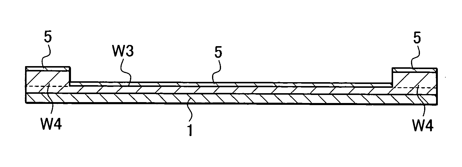
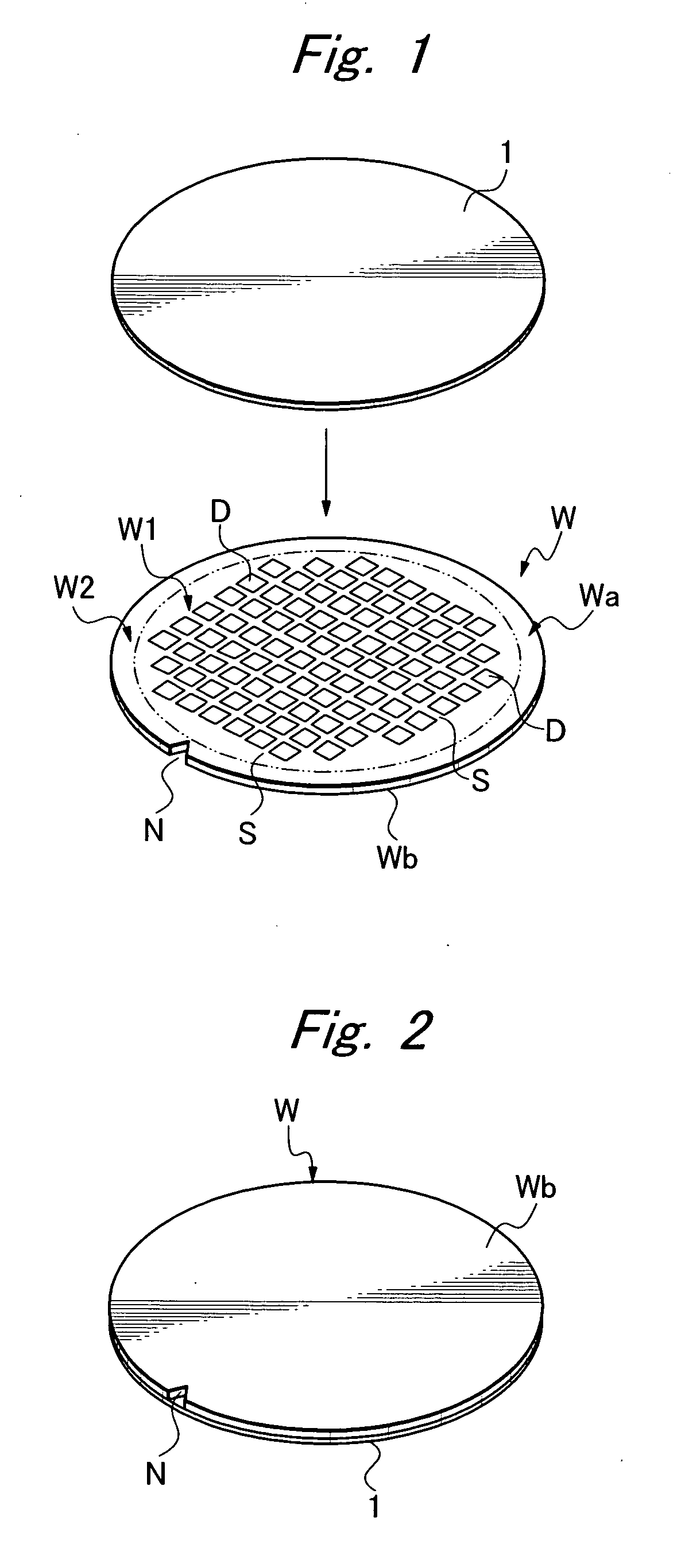
[0028] As shown in FIG. 1, in a surface Wa of a wafer W, a device region W1 having a plurality of devices D formed therein and a peripheral surplus region W2 enclosing the device region W1 are formed. In the device region W1, the devices D are formed by dividing streets S provided longitudinally and latitudinally. In a peripheral portion of the wafer W in a shown example, a notch N as a cutout indicating crystal orientation is formed.

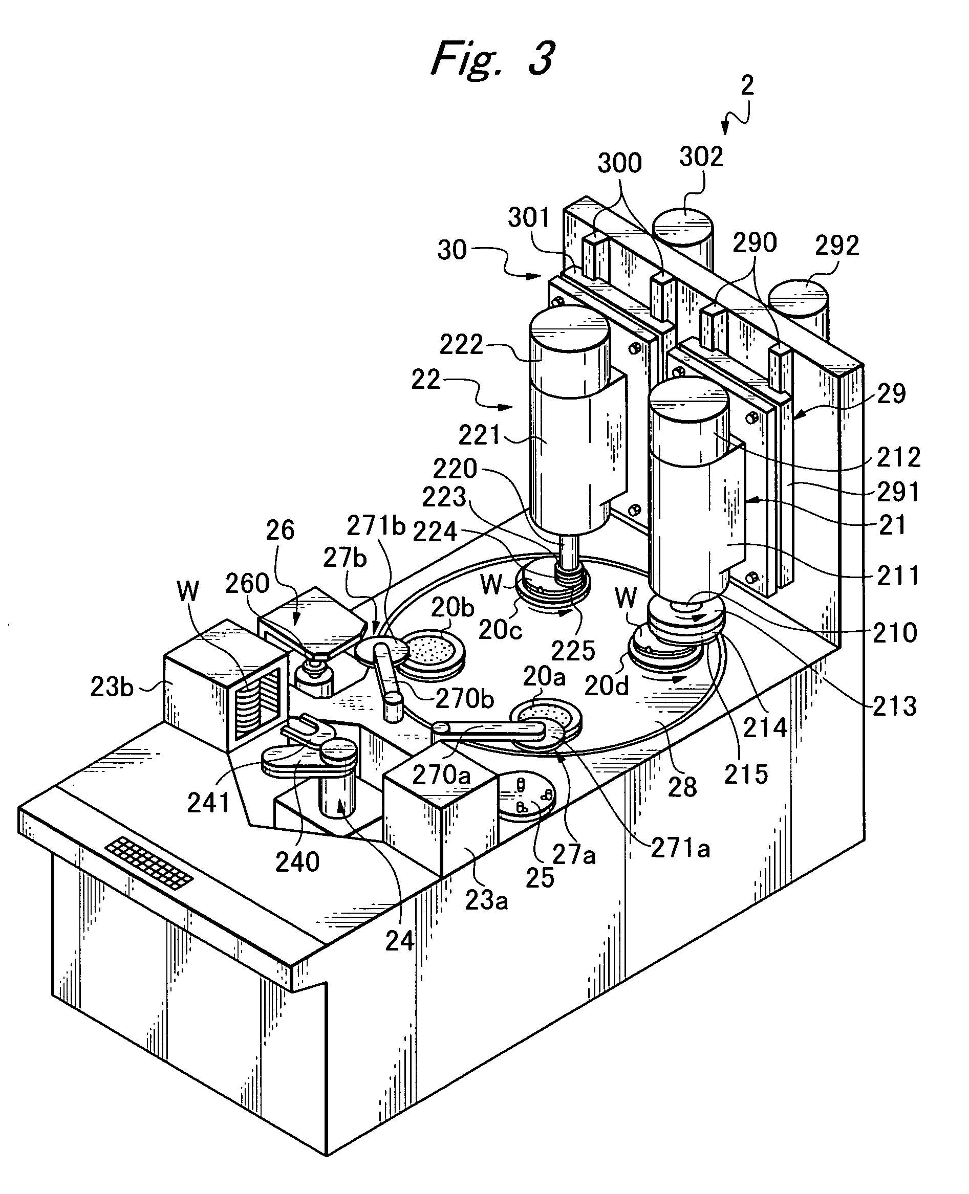
[0029] A protection member 1 such as tape is adhered on the surface Wa of the wafer 1 and then turned back to form a condition where the back Wb is exposed as shown in FIG. 2. Then, the back Wb is ground using a grinding apparatus 2 and the like as shown in FIG. 3.

[0030] The grinding apparatus 2 shown in FIG. 3 has chuck tables 20a, 20b, 20c and 20d of holding the wafer, a whole-back grinding unit 21 of grinding the whole back of a wafer held by each chuck table, and a device-region corresponding region grinding unit 22 of grinding a region correspond...


PUM

PropertyMeasurementUnit
thicknessaaaaaaaaaa
thicknessaaaaaaaaaa
thicknessaaaaaaaaaa

Abstract

To facilitate handling of a wafer in processing or carrying after the wafer being reduced in thickness by grinding, the whole back of a wafer having a surface on which a device region having a plurality of devices formed therein and a peripheral surplus region enclosing the device region are formed, is ground to be formed into a wafer having a predetermined thickness, and then a region corresponding to the device region in the back of the wafer is ground to form a concave portion having a predetermined thickness, so that a ring-like reinforcement portion is formed in a peripheral side of the concave portion, thereby the wafer is easily handled in a subsequent step or in wafer carrying between respective steps.

Description

BACKGROUND OF THE INVENTION [0001] 1. Field of the Invention [0002] The present invention relates to a wafer processing method in which a wafer is easily handled even if it is formed to be thin, and a grinding apparatus that can be used for performing the method. [0003] 2. Related Art [0004] A wafer on which a plurality of devices such as IC and LSI are formed on a surface side is divided into individual devices using a dicing machine, which are incorporated in various electronic devices and widely used. To achieve size reduction or weight saving of an electronic device, a wafer before dividing into individual devices is held at the surface side by a chuck table of a grinding apparatus for grinding a backside to be formed in a thickness of, for example, 20 μm to 100 μm (for example, refer to JP-A-2004-319885). SUMMARY OF THE INVENTION [0005] However, there is a difficulty that such a wafer formed thin by grinding loses stiffness and accordingly the wafer is hard to be handled or car...

Claims


Application Information

Patent Timeline
Patent Type & Authority Applications(United States)
IPC IPC(8): H01L21/30
CPCB24B7/228H01L21/304H01L21/02035
Inventor SEKIYA, KAZUMA
Owner DISCO CORP
Why Eureka
Try Eureka