

Circuit board and circuit apparatus using the same
a circuit board and circuit technology, applied in the field of circuit boards and circuit apparatuses, can solve the problems of reducing reliability, deteriorating reliability, and affecting the performance and reliability of circuit apparatuses, and achieve the effect of reducing reliability and increasing temperatur
- Summary
- Abstract
- Description
- Claims
- Application Information
AI Technical Summary
Benefits of technology
Problems solved by technology
Method used
Image

Examples
first embodiment
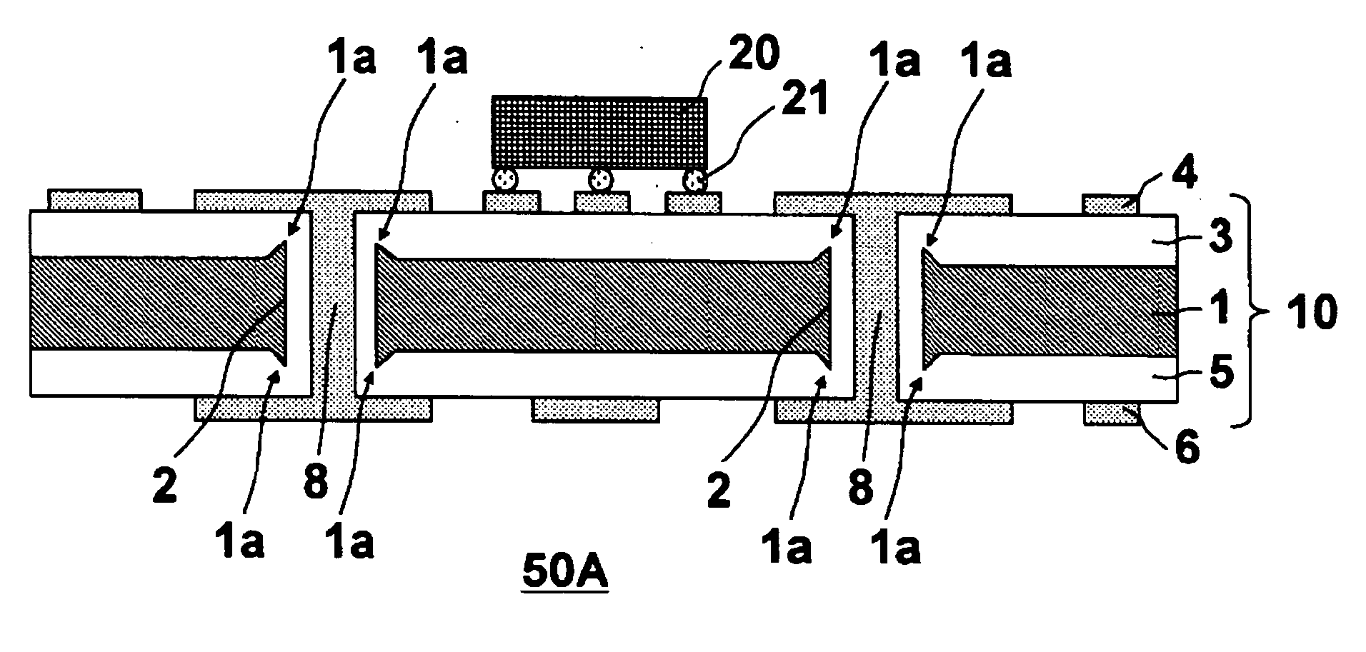
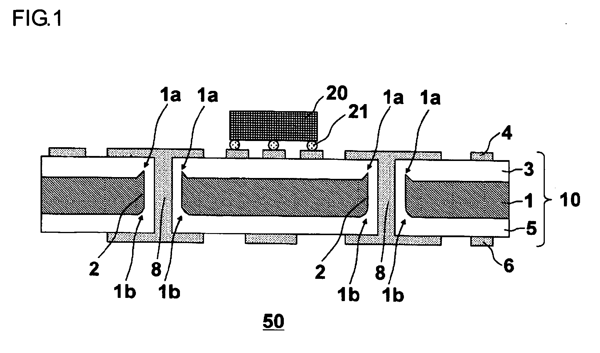
[0049]FIG. 1 is a sectional view of a circuit apparatus which has a circuit board including a metal substrate according to a first embodiment of the present invention.
[0050] According to the first embodiment of the present invention, the circuit apparatus 50 has a circuit board 10 in which a metal substrate 1, having a plurality of pierced holes 2, forms a core member. The metal substrate 1 has protrusions 1a at the top ends of the pierced holes 2, and rounded corners (depressions) 1b at the bottom ends of the pierced holes 2. Wiring pattern layers 4 and 6 are formed on both sides of this metal substrate 1 via insulating layers 3 and 5, respectively. In order to facilitate electrical connection between the wiring pattern layers, a conductor layer 8 for connecting the wiring pattern layer 4 and the wiring pattern layer 6 is formed through the metal substrate 1 via the pierced holes 2. The conductor layer 8 thereby establishes electrical conduction between the wiring pattern layers. ...
second embodiment
Modification of Second Embodiment
[0079]FIG. 8 shows a modification of the second embodiment shown in FIG. 7, in which protrusions are formed on both sides of the metal substrate.
[0080] In the second embodiment, the structure where the metal substrate 1 has protrusions 1a on both sides is achieved by forming the protrusions 1a at both ends of each of the pierced holes 2. In a modification of the second embodiment, the protrusions 1a are formed on either one end of each pierced hole 2 (depression 1b on the other end). In other words, some of the pierced holes 2 have their protrusions 1a on the top side of the metal substrate 1, and others have their protrusions 1a on the bottom side of the metal substrate 1. In other respects, the circuit apparatus in accordance with the modification of the second embodiment has the same configuration as in the second embodiment.
[0081] The circuit apparatus in accordance with this modification of the second embodiment can also provide the foregoing ...
third embodiment
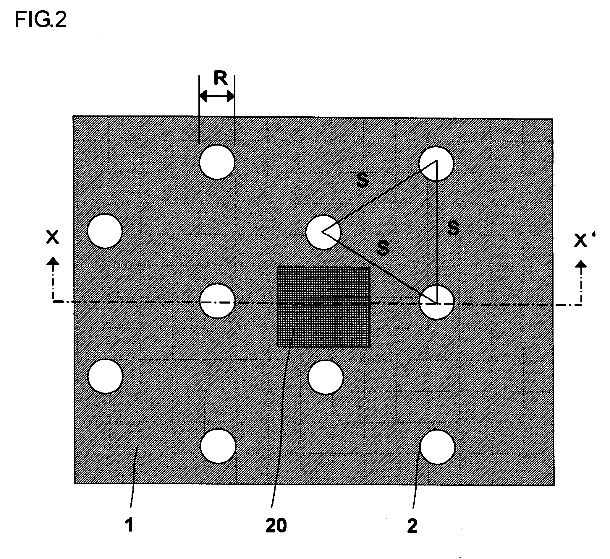
[0082]FIG. 9 is a plan view showing the positions of pierced holes formed in the metal substrate of a circuit apparatus according to a third embodiment of the present invention. FIG. 10 is a schematic sectional view of the circuit apparatus, taken along the line X-X′ of FIG. 9. Differences from the first embodiment consist in the following two points. First, the pierced holes 2 (diameter R: approximately 300 μm) piercing through the metal substrate 1 are formed in a honeycomb configuration of higher density (S=2R, where S is the pitch between pierced holes). Second, the plurality of pierced holes includes pierced holes 2a that are provided with the conductor layer 8 and pierced holes (dummy pierced holes) 2b that are not provided with the conductor layer 8. In other respects, the circuit apparatus in accordance with the third embodiment is the same as that of the foregoing first embodiment.
[0083] Specifically, in the foregoing step shown in FIG. 4B, the laser irradiation or drillin...
PUM
| Property | Measurement | Unit |
|---|---|---|
| Density | aaaaa | aaaaa |
| Volume | aaaaa | aaaaa |
| Area | aaaaa | aaaaa |
Abstract
Description
Claims
Application Information