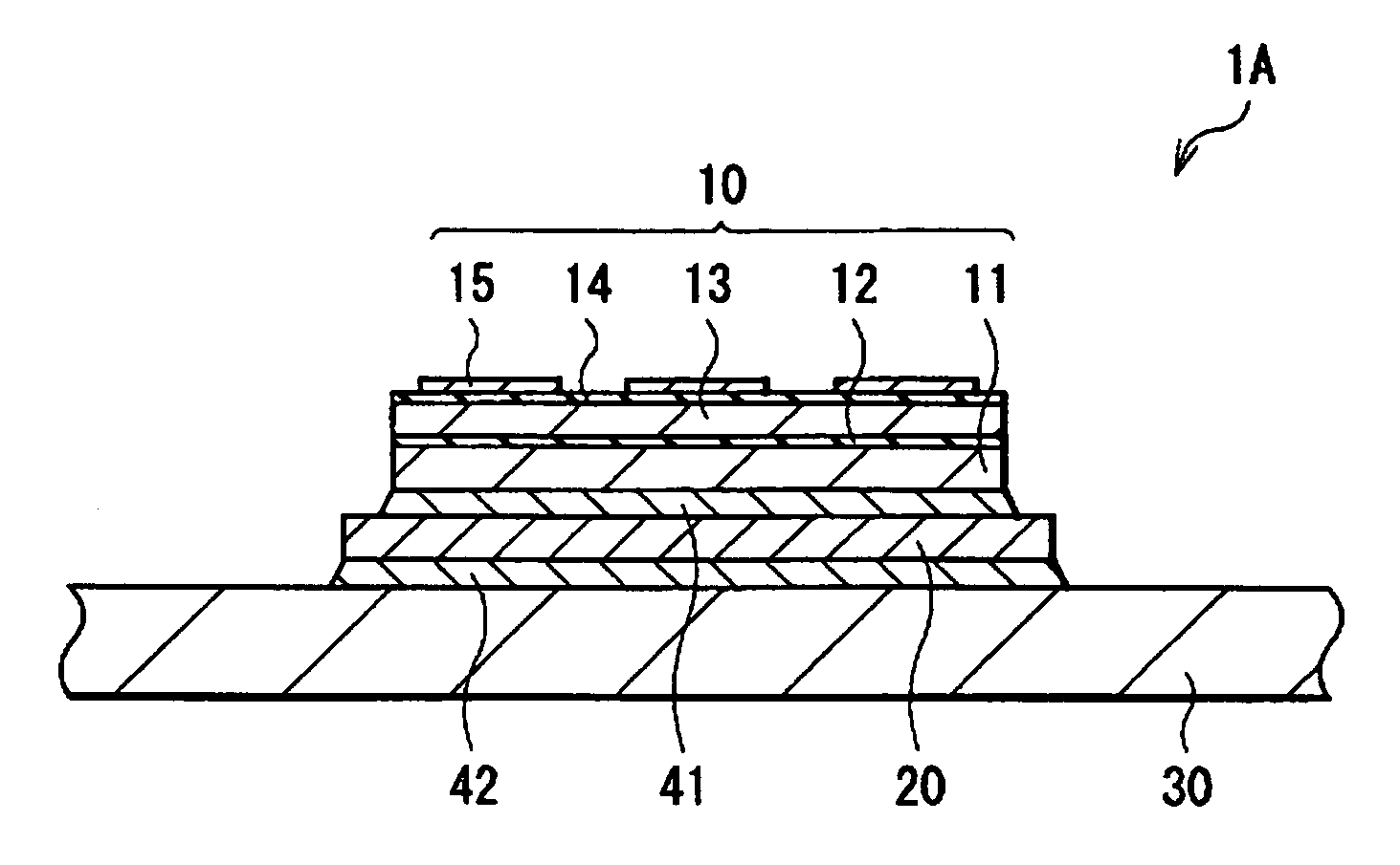
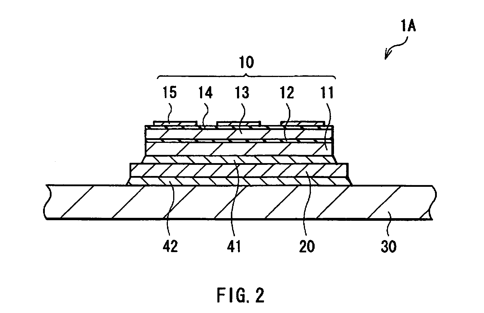
[0009] In the thin film device, the thin film element is disposed on a surface of the substrate for high
voltage exhibiting an
electric resistivity in the range of 108Ω·cm to 1010Ω·cm, with the conductive adhesive layer in between. Therefore, if electric charges are generated in the thin film element, these electric charges can be discharged gradually, instead of being accumulated in large amounts, via the conductive adhesive layer to the substrate for high
voltage. This enables suppression of ESD, while ensuring a sufficient
dielectric breakdown voltage.
[0011] In the thin film device module, the thin film element is disposed on a surface of the substrate for high voltage exhibiting an
electric resistivity in the range of 108Ω·cm to 1010Ω·cm, with the first conductive adhesive layer in between, and the conductive substrate is disposed on a surface of the opposite side of the substrate for high voltage, with the second conductive adhesive layer in between. Therefore, if electric charges are generated in the thin film element, these electric charges can be discharged gradually, instead of being accumulated in large amounts, via these conductive adhesive
layers to the substrate for high voltage. This enables suppression of ESD, while ensuring sufficient
dielectric breakdown voltage between the conductive substrate and the thin film element.
[0013] In the method of forming a thin film device, the thin film device is formed by disposing the thin film element on a surface of the substrate for high voltage exhibiting an electric resistivity in the range of 108Ω·cm to 1010Ω·cm, with the first conductive adhesive layer in between, and the thin film device is disposed on the conductive substrate, with the second conductive adhesive layer in between. Therefore, if electric charges are generated in the thin film element, the electric charges can be discharged gradually, instead of being accumulated in large amounts, via these conductive adhesive
layers to the substrate for high voltage. This enables suppression of ESD, while ensuring a sufficient dielectric breakdown voltage between the conductive substrate and the thin film element.
[0015] In the thin film device of an embodiment of the present invention, the thin film element is disposed on a surface of the substrate for high voltage exhibiting an electric resistivity in the range of 108Ω·cm to 1010Ω·cm, with the conductive adhesive layer in between. Therefore, if electric charges are generated in the thin film element, ESD can be suppressed by allowing these electric charges, while they are not accumulated in large amounts, to shift gradually via the conductive adhesive layer to the substrate for high voltage. On the other hand, even when disposed on the conductive substrate, it is possible to ensure a sufficient dielectric breakdown voltage. Hence, the thin film device is less susceptible to damage due to ESD, and has superior withstand voltage characteristic to permit a stable operation.
[0016] In the thin film device module of an embodiment of the present invention, the thin film element is disposed on a surface of the substrate for high voltage exhibiting an electric resistivity in the range of 108Ω·cm to 1010Ω·cm, with the first conductive adhesive layer in between, and the conductive substrate is disposed on a surface of the opposite side of the substrate for high voltage, with the second conductive adhesive layer in between. Therefore, if electric charges are generated in the thin film element, ESD can be suppressed by allowing the electric charges, while they are not accumulated in large amounts, to shift gradually via these conductive adhesive
layers to the substrate for high voltage. On the other hand, it is also possible to ensure a sufficient dielectric breakdown voltage between the conductive substrate and the thin film device. Hence, the thin film device module is less susceptible to damage due to ESD, and has superior withstand voltage characteristic to permit a stable operation.
[0017] In the method of forming a thin film device module of an embodiment of the present invention, after forming the thin film device by disposing the thin film element on the substrate for high voltage exhibiting an electric resistivity in the range of 108Ω·cm to 1010Ω·cm, with the first conductive adhesive layer in between, the thin film device is disposed on a conductive substrate, with the second conductive adhesive layer in between. Therefore, if electric charges are generated in the thin film element, ESD can be suppressed by allowing the electric charges, while they are not accumulated in large amounts, to shift gradually via the conductive adhesive layer to the substrate for high voltage. Further, it is possible to ensure a sufficient dielectric breakdown voltage between the conductive substrate and the thin film device. Hence, it is easy to attain a thin film device module that is less susceptible to damage due to ESD, and has superior withstand voltage characteristic to permit a stable operation.



