
Thin film device, thin film device module, and method of forming thin film device module

a thin film device and module technology, applied in the direction of superconductor devices, instruments, basic electric elements, etc., can solve the problem of not concluding that the insulating property of the thin film device is guaranteed, and achieve the effects of reducing the risk of damag

Inactive Publication Date: 2008-04-08
TDK CORPARATION
View PDF5 Cites 0 Cited by
  • Summary
  • Abstract
  • Description
  • Claims
  • Application Information

AI Technical Summary

Benefits of technology

The present invention provides a thin film device that is less susceptible to damage due to ESD and has superior withstand voltage characteristic to permit a stable operation. This is achieved by improving the insulating properties of the thin film device by using a substrate for high voltage with an electric resistivity in the range of 108 Ω·cm to 1010 Ω·cm and a conductive adhesive layer in between. The thin film element is disposed on the substrate for high voltage with a conductive adhesive layer in between, and the conductive substrate is disposed on the opposite side of the thin film element with another conductive adhesive layer in between. This allows the electric charges generated in the thin film element to be gradually discharged via the conductive adhesive layers to the substrate for high voltage, suppressing ESD and ensuring a sufficient dielectric breakdown voltage between the conductive substrate and the thin film element. The method of forming a thin film device module using this substrate and conductive adhesive layers is also provided.

Problems solved by technology

Consequently, it should not be concluded that sufficient insulating property of the thin film device is ensured.

Method used


Image

  • Thin film device, thin film device module, and method of forming thin film device module
  • Thin film device, thin film device module, and method of forming thin film device module
  • Thin film device, thin film device module, and method of forming thin film device module

Examples


examples

[0046]The following is examples of the present invention.

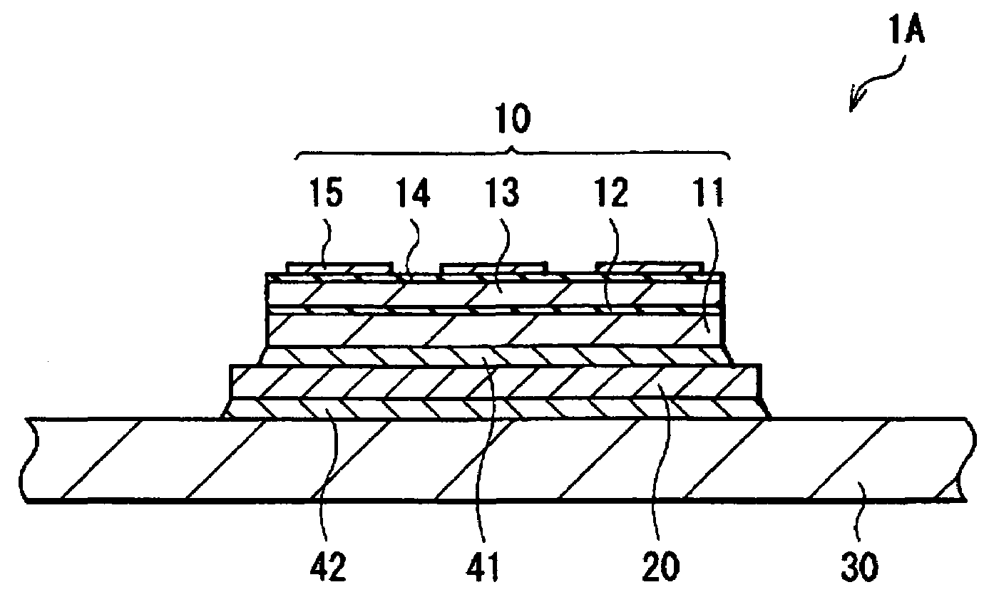
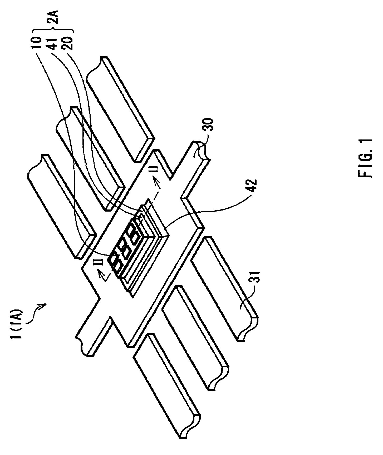
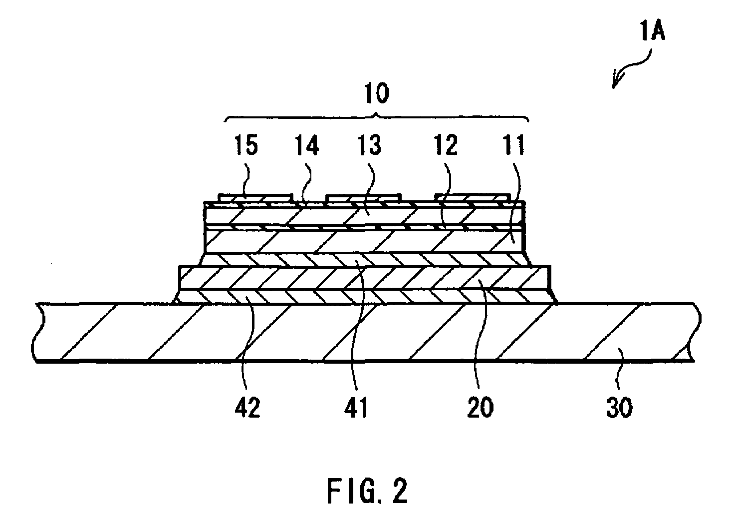
[0047]In the examples, samples corresponding to the module 1A as shown in FIGS. 1 and 2 were prepared, and their respective dielectric breakdown voltages were measured.

[0048]That is, the measurements were made with the sample immersed in an oil bath, while changing an applied voltage (kV) with the passage of time (second) in accordance with the profile as shown in FIG. 5. The maximum applied voltage was 15 kV.

[0049]FIG. 6 shows the results of the measurements of the dielectric breakdown voltages of the substrate for high voltage 20. In FIG. 6, the abscissa represents an applied voltage, and the ordinate represents the resistance of the module as a whole. In these examples, the thickness of the substrate for high voltage 20 had three levels of 80 μm, 150 μm, and 300 μm, which were designated by T80, T150, and T300, respectively. As a result, the dielectric breakdown voltage was 5 kV when the thickness was 80 μm, 11 kV when it w...


PUM

PropertyMeasurementUnit
electric resistivityaaaaaaaaaa
dielectric breakdown voltageaaaaaaaaaa

Abstract

A thin film device includes a thin film element disposed on a surface of a substrate for high voltage formed of a material having an electric resistivity in the range of 108 Ω·cm to 1010 Ω·cm, with an adhesive layer in between. The substrate for high voltage is a sintered body containing Al2O3, TiC, and MgO in a predetermined weight ratio. Therefore, if electric charges are generated in the thin film element, the electric charges are, while they are not accumulated in large amounts, gradually shifted via the adhesive layer to the substrate for high voltage, so that the generation of ESD can be suppressed. On the other hand, even when mounted on a lead frame, a sufficient dielectric breakdown voltage can be ensured. This provides a thin film device that is less susceptible to damage due to ESD, and has superior withstand voltage characteristic to permit a stable operation.

Description

BACKGROUND OF THE INVENTION[0001]1. Field of the Invention[0002]The present invention relates to a thin film device having a thin film element functioning electrically or magnetically, and a thin film device module provided with a thin film device, as well as a method of forming a thin film device module.[0003]2. Description of the Related Art[0004]In general, a semiconductor device or a thin film device having a functional film such as a magnetic sensor is secured with adhesive to a conductive substrate such as a lead frame. For example, as shown in FIG. 8, a thin film device 120, which includes a functional film 123 disposed on a surface of a conductive substrate 121 of silicon (Si) or the like with an insulating film 122 in between, is fixed to a lead frame 130 with an adhesive layer 140 in between. Typically, however, the adhesive layer 140 is an insulator and therefore electric charge is apt to accumulate in the functional film 123, so that its surface potential may rise moment...

Claims


Application Information

Patent Timeline
Patent Type & Authority Patents(United States)
IPC IPC(8): H01L23/58
CPCB82Y25/00G01R33/093H01L43/02H01L2224/32245H10N50/80
Inventor SHOJI, SHIGERU
Owner TDK CORPARATION
Learn More