Liquid crystal display device

a liquid crystal display and display device technology, applied in non-linear optics, instruments, optics, etc., can solve the problems of excessive brightening of images, deteriorating contrast ratio, and oblique deterioration of the reproductivity of the gray scal

Active Publication Date: 2007-02-01
PANASONIC LIQUID CRYSTAL DISPLAY CO LTD +1
View PDF6 Cites 93 Cited by
  • Summary
  • Abstract
  • Description
  • Claims
  • Application Information

AI Technical Summary

Problems solved by technology

The VA type liquid crystal display device has suffered from such a problem that the gray scale reproductivity is deteriorated in the oblique direction.
Also, in the VA type liquid crystal display device of the transflective type, since black display is also shifted to the higher tone side in addition to the halftone, the contrast ratio is deteriorated in addition to the excessively brightened image.
On the other hand, the ECB type liquid crystal display device suffers from such a problem that the azimuth dependency of the viewing performance is large.
However, since the slope direction of the liquid crystal layer is not uniform, the tone shift eliminating method of the oblique direction using the liquid crystal polymer film such as the ECB type liquid crystal display device is not effected.
However, since those methods are complicated in the pixel structure and insufficient in the di

Method used


Image

  • Liquid crystal display device
  • Liquid crystal display device
  • Liquid crystal display device

Examples


first embodiment

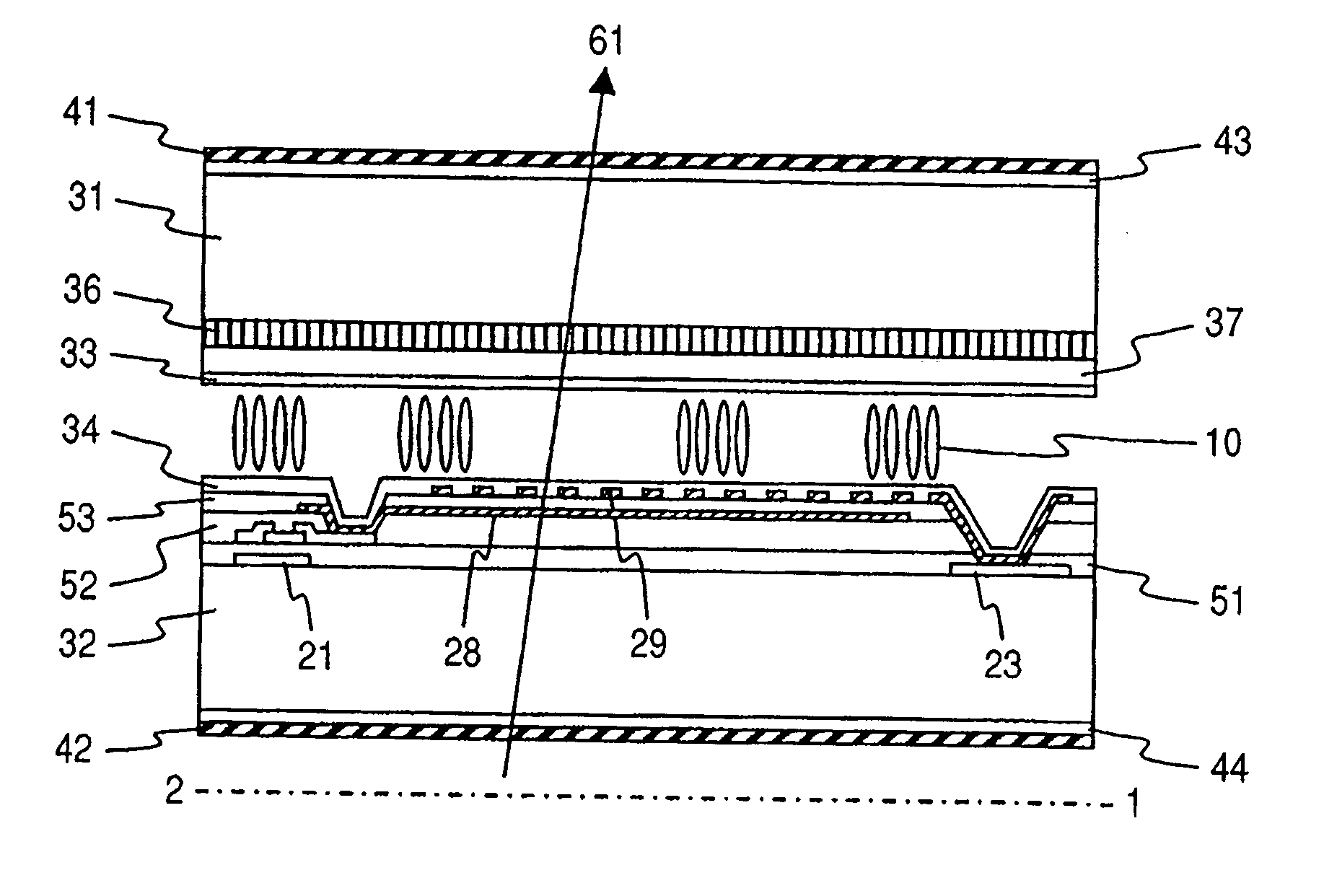
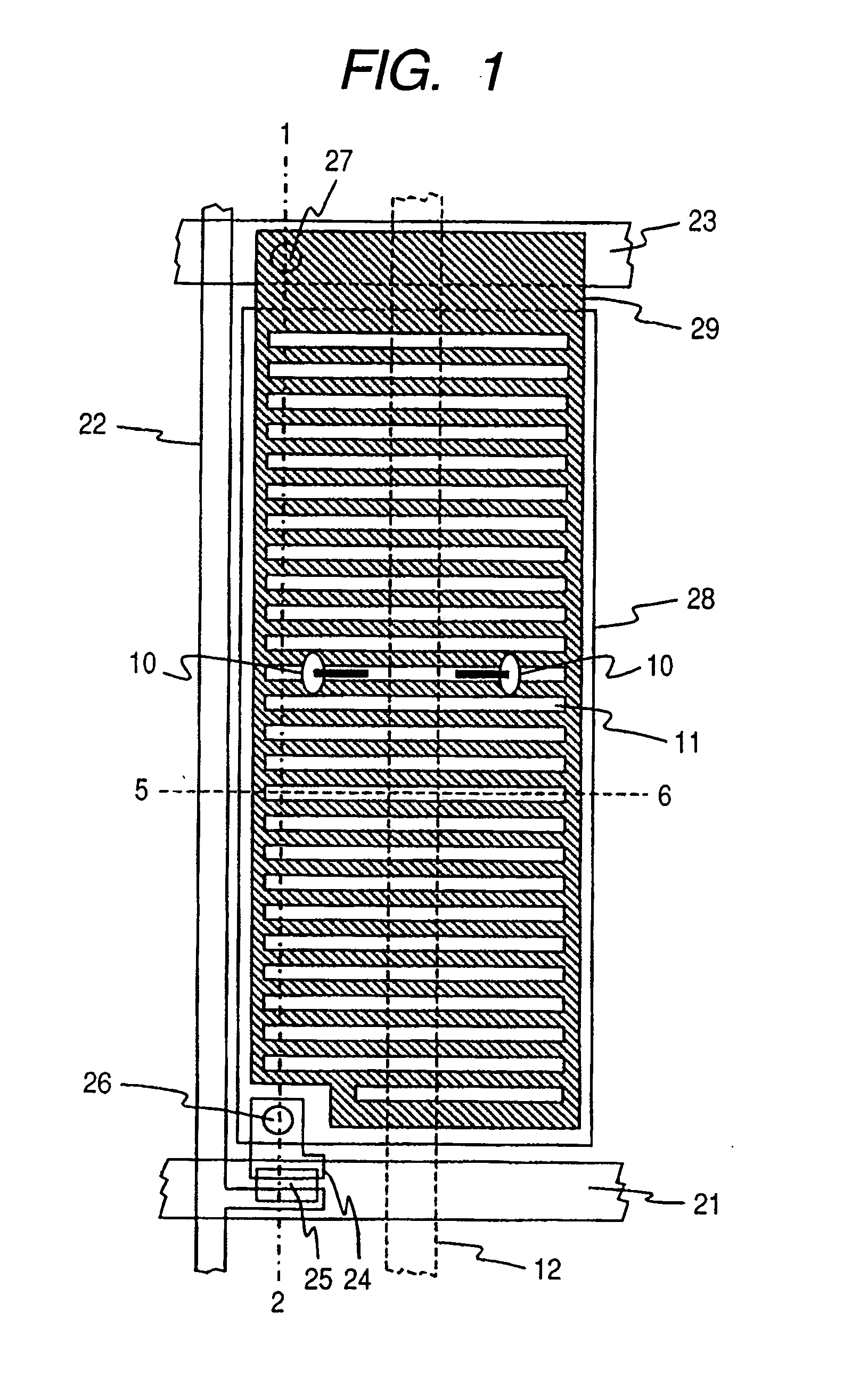
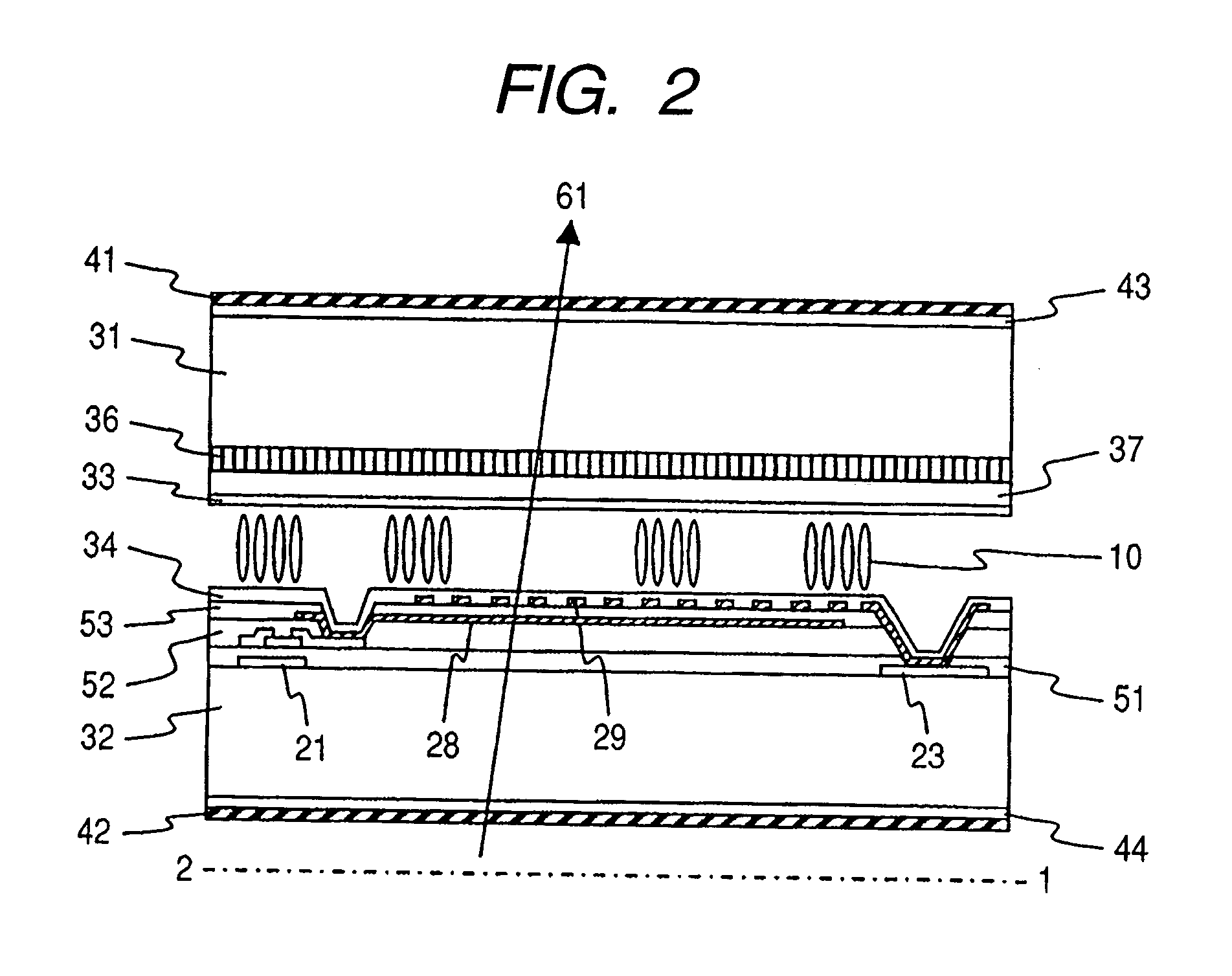
[0070]FIG. 2 shows a cross-sectional view of one pixel that constitutes a liquid crystal display device according to the present invention (a cross-sectional view taken along a chain line shown in FIG. 1), and FIG. 1 shows a top view of a second substrate 32 viewed from a normal direction. FIG. 1 mainly shows a plan distribution of a formation of the second substrate side 32. Only alignment control structure 12 indicated by a broken line is shown by the formation of a first substrate side 31. Also, FIG. 1 shows plural lines and plural electrodes. Because those lines and electrodes are not always flush, they are so distributed as to be partially overlapped with each other. One of those electrodes which is closest to a liquid crystal layer is hatched.

[0071] The liquid crystal display device according to the present invention mainly includes a first substrate 31, a liquid crystal layer 10, and a second substrate 32. The first substrate 31 and the second substrate 32 sandwich the liqui...

second embodiment

[0108] In the first embodiment, as shown in FIG. 1, the alignment control structure 12 is disposed in parallel to the longer side direction of one pixel. In this case, a distance between the alignment control structure 12 and the liquid crystal layer within a pixel which is farthest from the alignment control structure 12, that is, the liquid crystal layer at the end of the pixel which is close to the signal line 22 is short, and the liquid crystal alignment control effect due to the alignment control structure 12 is liable to be influenced on one entire pixel.

[0109] On the contrary, in this embodiment, as shown in FIG. 7, the boundary of two domains is disposed in parallel to the shorter side direction of one pixel. More specifically, the direction of the slits 11 is set to be in parallel to the signal line 22, and the alignment control structure 12 is disposed in parallel to the scanning line 21, and passes through the center of one pixel. Even in this case, the same oblique char...

third embodiment

[0114] In this embodiment, both of the common electrode 29 and the pixel electrode 28 are of the comb-like planar structure, and formed in the same layer. FIG. 8 shows a plan structure of one pixel of the liquid crystal display device according to this embodiment. The pixel electrode 28 is hatched as with the common electrode 29, and its comb-like structure is disposed in parallel to the signal line 22.

[0115] The common electrode 29 is disposed in the vicinity of the signal line 22, and has a function of shielding the signal line potential. A surface of the first substrate 31 in proximity to the liquid crystal layer 10 disposes the alignment control structure 12. The alignment control structure 12 is of the stripe-like plan structure as in the second embodiment, and the stripe is disposed in parallel to the scanning line 21, and distributed so as to divide one pixel into two equal parts. The lines of electric force are formed in an arch between the common electrode 29 and the pixel...


PUM


Abstract

AVA liquid crystal display device is capable of performing display under the wide environments including a bright place and a dark place, transmission display with a wide viewing angle and a high image quality, and improves the gray scale productivity in an oblique direction. An alignment control structure (projection structure) is disposed in a direction orthogonal to the slits of a common electrode (comb-like electrode), a lateral electric field is applied to a liquid crystal layer that is vertically aligned by the comb-like electrode, and the alignment of the liquid crystal is controlled to a different direction to make multi-domains in the VA liquid crystal display device. Also, the multi-domains are performed by continuously changing the pitches of the slits.

Description

CLAIM OF PRIORITY [0001] The present application claims priority from Japanese Application JP 2005-220533 filed on Jul. 29, 2005, the content of which is hereby incorporated by reference into this application. BACKGROUND OF THE INVENTION [0002] 1. Field of the Invention [0003] The present invention relates to a liquid crystal display device that divides a liquid crystal layer that is vertically aligned in multiple domains. [0004] 2. Description of the Related Art [0005] Presently, a transmission type liquid crystal display device of a wide viewing angle such as an IPS (In Plane Switching) type or a VA (Vertical Alignment) type has been spread as a monitor, has improved the response characteristic, and has been used as a television. The liquid crystal display device for the television has been increasingly enlarged in the screen, and there is a case in which plural users watch the large-screen liquid crystal display device at the same time. Under the circumstances, it is desirable to...

Claims


Application Information

Patent Timeline
IPC IPC(8): G02F1/1343G02F1/1337
CPCG02F1/134363G02F2001/134372G02F2001/134318G02F1/134318G02F1/134372
Inventor ITOU, OSAMUADACHI, MASAYAOKA, SHINICHIRO
Owner PANASONIC LIQUID CRYSTAL DISPLAY CO LTD
Why Eureka
Try Eureka