

Magnetoresistive device and nonvolatile magnetic memory equipped with the same
- Summary
- Abstract
- Description
- Claims
- Application Information
AI Technical Summary
Benefits of technology
Problems solved by technology
Method used
Image

Examples
example 1
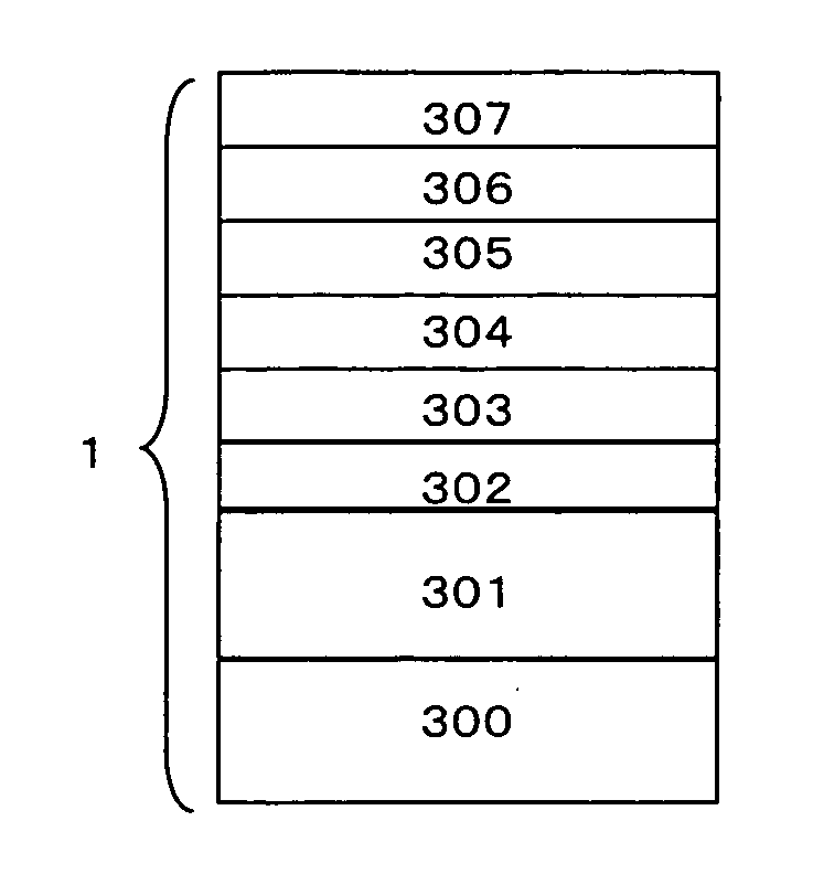
[0028]FIG. 1 shows a schematic cross section of an example of a tunnel magnetoresistive device of the invention. A tunnel magnetoresistive device 1 is formed by stacking an orientation control film 300, an antiferromagnetic film 301, a ferromagnetic film 302, a non-ferromagnetic film 303, a ferromagnetic film 304, an insulator film 305, a ferromagnetic film 306, and a protection film 307. The device is thermally processed at an appropriate temperature so as to optimize its magnetoresistance ratio. The tunnel magnetoresistive device according to the present embodiment was prepared by a sputtering process.
[0029] While the orientation control film 300 was formed from NiFe (5 nm), other material may be used that are capable of improving the orientation of the aforementioned antiferromagnetic film 301 and achieving stable anti-ferromagnetic coupling, such as a double-layer film of Ta (5 nm) / NiFe (5 nm), for example. While the antiferromagnetic film 301 employed MnIr (8 nm), the film thi...
example 2
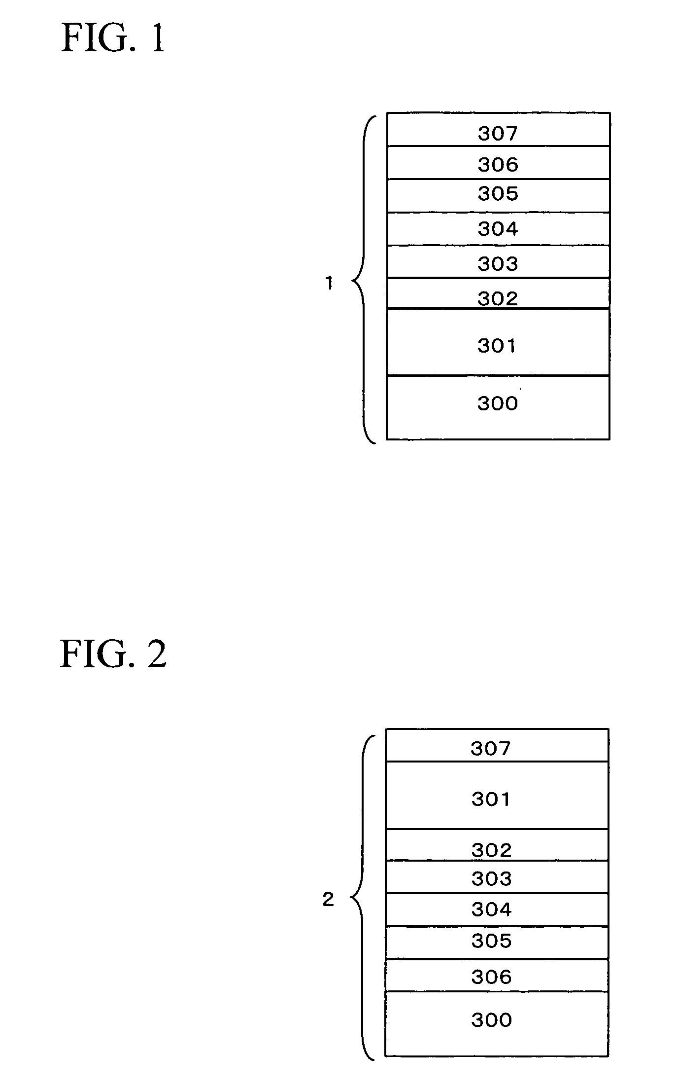
[0035]FIG. 2 shows a schematic cross section of another example of the tunnel magnetoresistive device of the invention. A tunnel magnetoresistive device 2 was formed by stacking an orientation control film 300, a ferromagnetic film 306, an insulator film 305, a ferromagnetic film 304, a non-ferromagnetic film 303, a ferromagnetic film 302, an antiferromagnetic film 301, and a protection film 307. In particular, when CoFeB is used in the ferromagnetic film 306 and the ferromagnetic layer film 304, the resultant crystal structure is a body center cubic. The insulator film 305 is MgO having a rock-salt structure highly oriented in (100).
[0036] In the tunnel magnetoresistive device 2 of the present example, because the ferromagnetic film 306 is formed adjacent to the oriented insulator film 300 and has an excellent flatness, the soft magnetic property of the ferromagnetic film 306 can be improved over that of the structure according to Example 1. For example, the coercivity of CoFeB af...
example 3
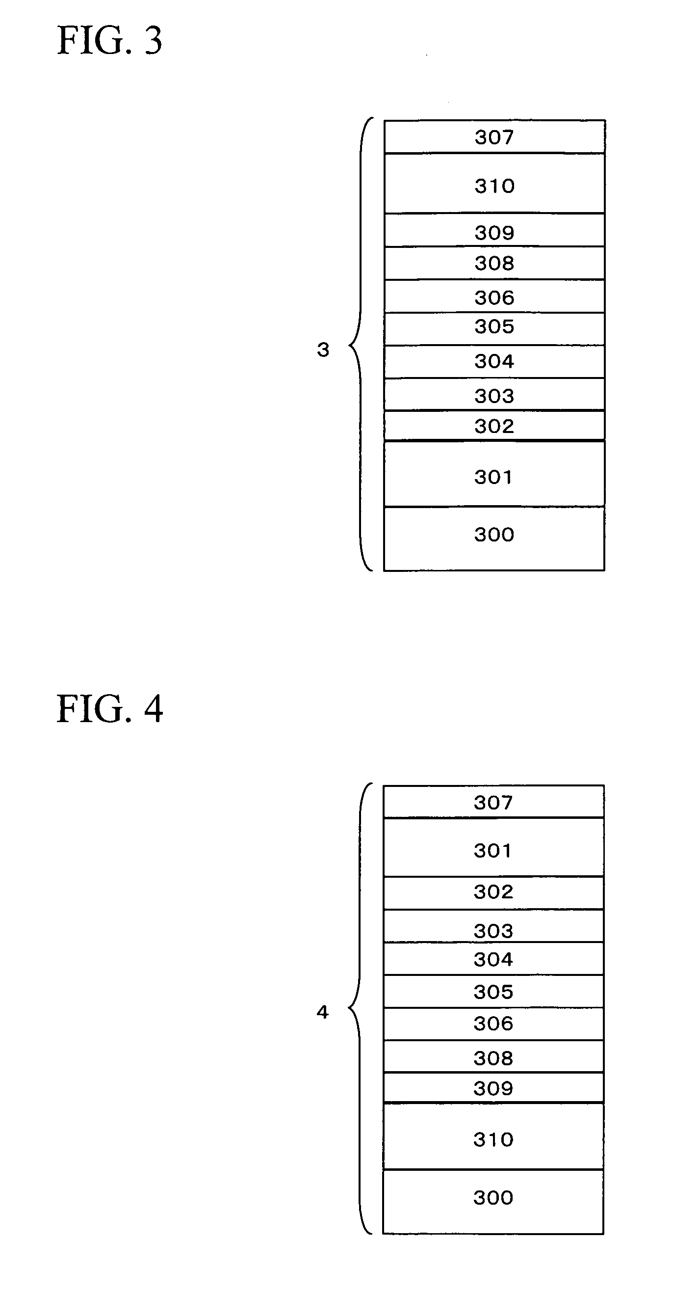
[0037]FIG. 3 shows a schematic cross section of another example of the tunnel magnetoresistive device of the invention. The structure of the tunnel magnetoresistive device 3 is similar to that of the tunnel magnetoresistive device 1 shown in FIG. 1 with the exception that, on the ferromagnetic film 306, a non-ferromagnetic film 308, a ferromagnetic film 309, an antiferromagnetic film 310, and a protection film 307 were stacked sequentially in mentioned order.
[0038] In the present example, Ru (6 nm) was used in the non-ferromagnetic film 308, CoFe (2 nm) was used in the ferromagnetic film 309, and MnIr (8 nm) was used in the antiferromagnetic film 310. The composition ratio of CoFe of the ferromagnetic film 309 was selected such that the Co composition ranged between 50 to 90%, at which a stable anti-ferromagnetic coupling can be realized between the ferromagnetic film 309 and the antiferromagnetic film 310. For the non-ferromagnetic film 308, a material or film thickness other than...
PUM
 Abstract
Description
Claims
Application Information