

Operating method for a large dimension plasma enhanced atomic layer deposition cavity and an apparatus thereof
a plasma enhanced atomic layer and cavity technology, applied in the field of operating methods and apparatuses thereof, can solve the problems of low element reliability, high leakage current, and pressure rise, and achieve enhanced atomic layer deposition cavity, effective pressure control, and increased gas-flow
- Summary
- Abstract
- Description
- Claims
- Application Information
AI Technical Summary
Benefits of technology
Problems solved by technology
Method used
Image

Examples
Embodiment Construction
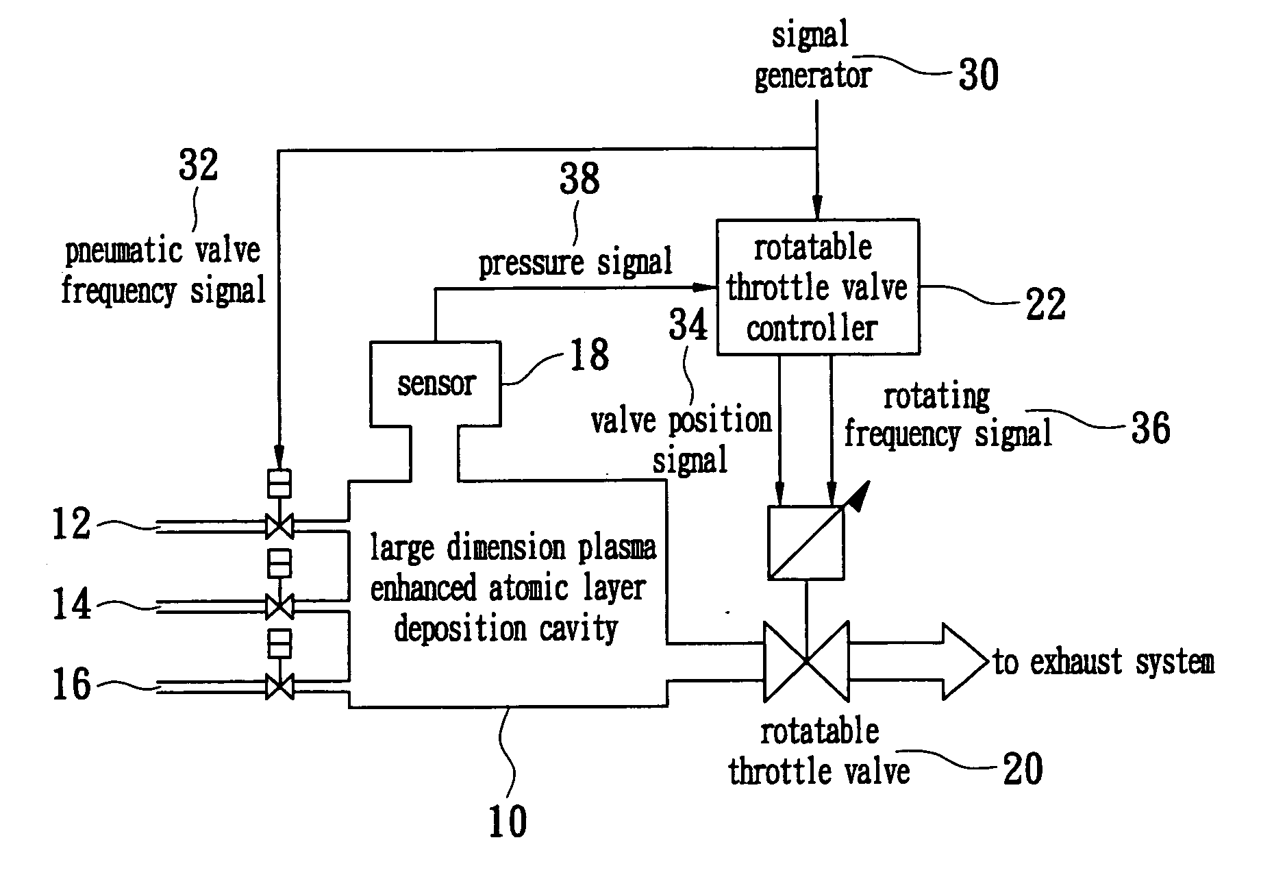
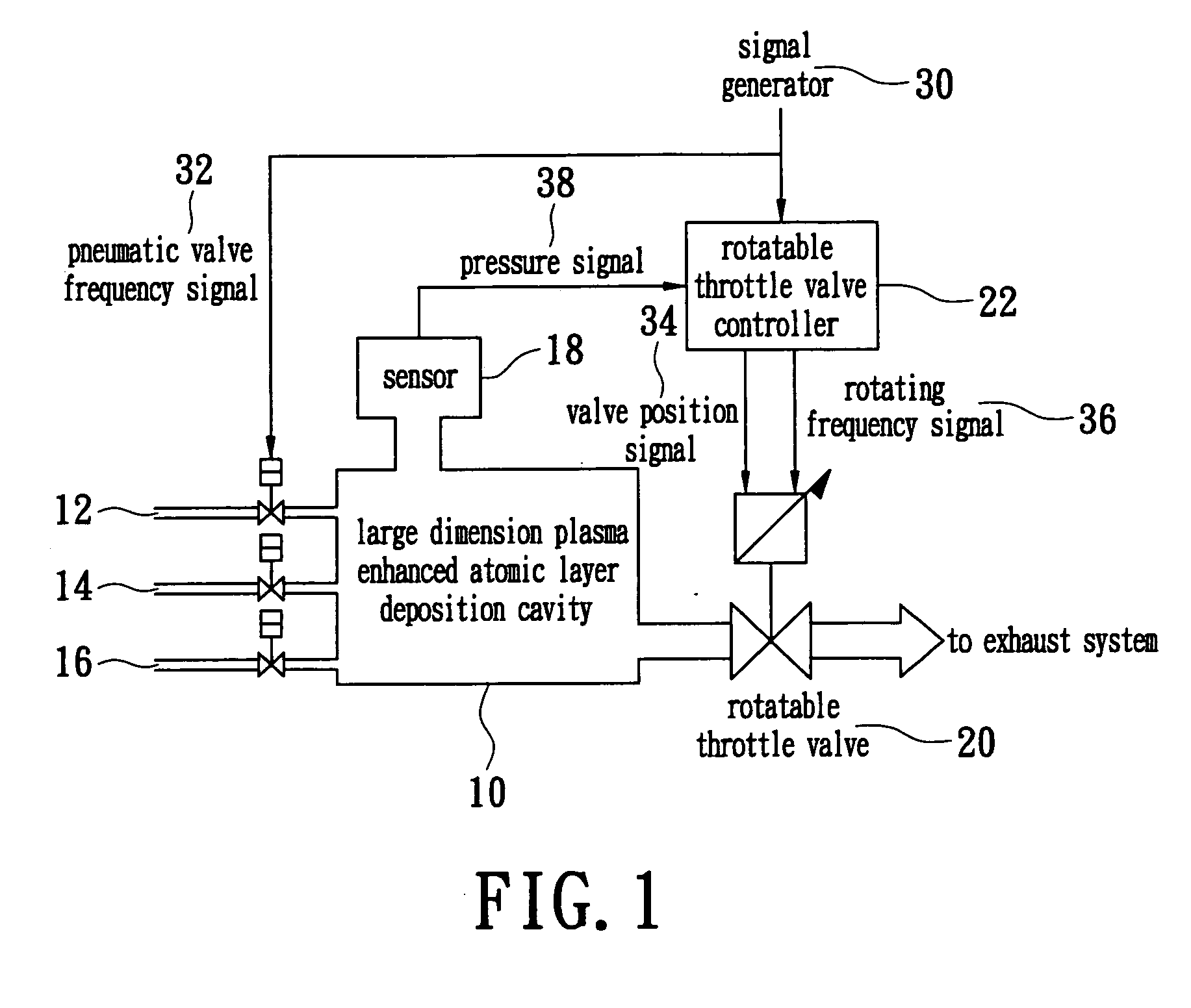
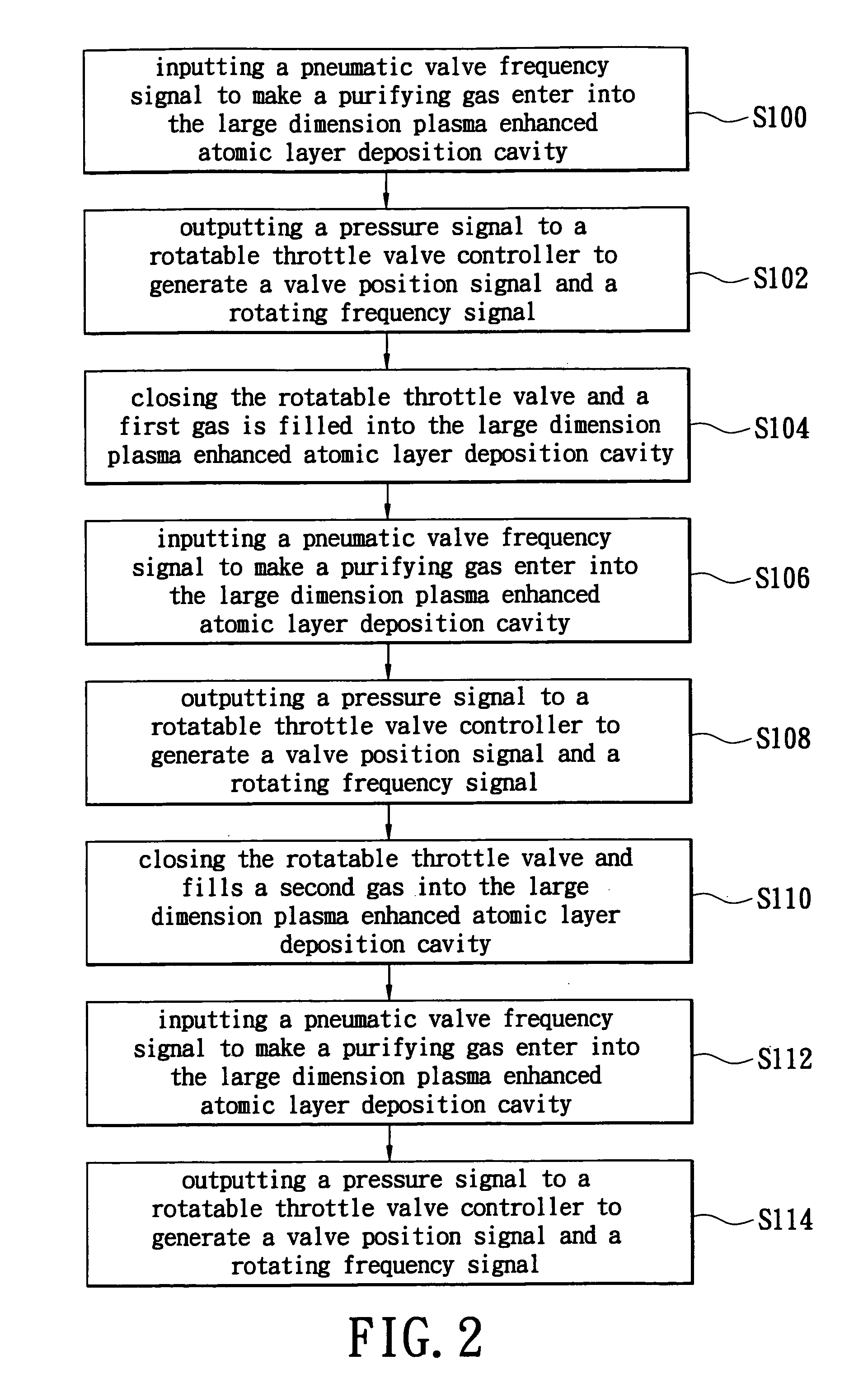
[0033] Reference is made to FIG. 1. FIG. 1 shows a schematic view of the apparatus of a large dimension plasma enhanced atomic layer deposition cavity of the present invention. The apparatus of a large dimension plasma enhanced atomic layer deposition cavity includes a large dimension plasma enhanced atomic layer deposition cavity 10, a first gas supply source 12, a second gas supply source 14, a purifying gas supply source 16 and a sensor 18, a rotatable throttle valve 20 and a rotatable throttle valve controller 22. The large dimension plasma enhanced atomic layer deposition cavity 10 defines a reaction space. The first gas supply source 12 is connected to one side of the large dimension plasma enhanced atomic layer deposition cavity 10 for providing a first gas. The second gas supply source 14 is connected to one side of the large dimension plasma enhanced atomic layer deposition cavity 10 for providing a second gas. The purifying gas supply source 16 is connected to one side of ...
PUM
| Property | Measurement | Unit |
|---|---|---|
| frequency | aaaaa | aaaaa |
| pressure | aaaaa | aaaaa |
| dimension | aaaaa | aaaaa |
Abstract
Description
Claims
Application Information