High voltage non punch through IGBT for switch mode power supplies

a high-voltage, switch-mode power supply technology, applied in the direction of transistors, electrical appliances, semiconductor devices, etc., can solve the problem that devices are not well adapted to the application of switch-mode power supplies

Active Publication Date: 2007-02-01
INFINEON TECH AMERICAS CORP
View PDF4 Cites 12 Cited by
  • Summary
  • Abstract
  • Description
  • Claims
  • Application Information

AI Technical Summary

Benefits of technology

[0005] In accordance with the present invention a novel NPT IGBT is produced in a thinned wafer (less than about 100 μ thick) having a P+ transparent anode (collector) at its bottom, and a novel low lifetime region adjacent the transparent anode to control switching loss. The low lifetime region is formed by an implant of a light atomic species, preferably hydrogen, which has previously been used only for punch through devices.

Problems solved by technology

Such devices are not well adapted to application to switch mode power supplies in which the turn off energy EOFF is to be minimized, even at the expense of a higher VCEON.

Method used


Image

  • High voltage non punch through IGBT for switch mode power supplies
  • High voltage non punch through IGBT for switch mode power supplies

Examples


first embodiment

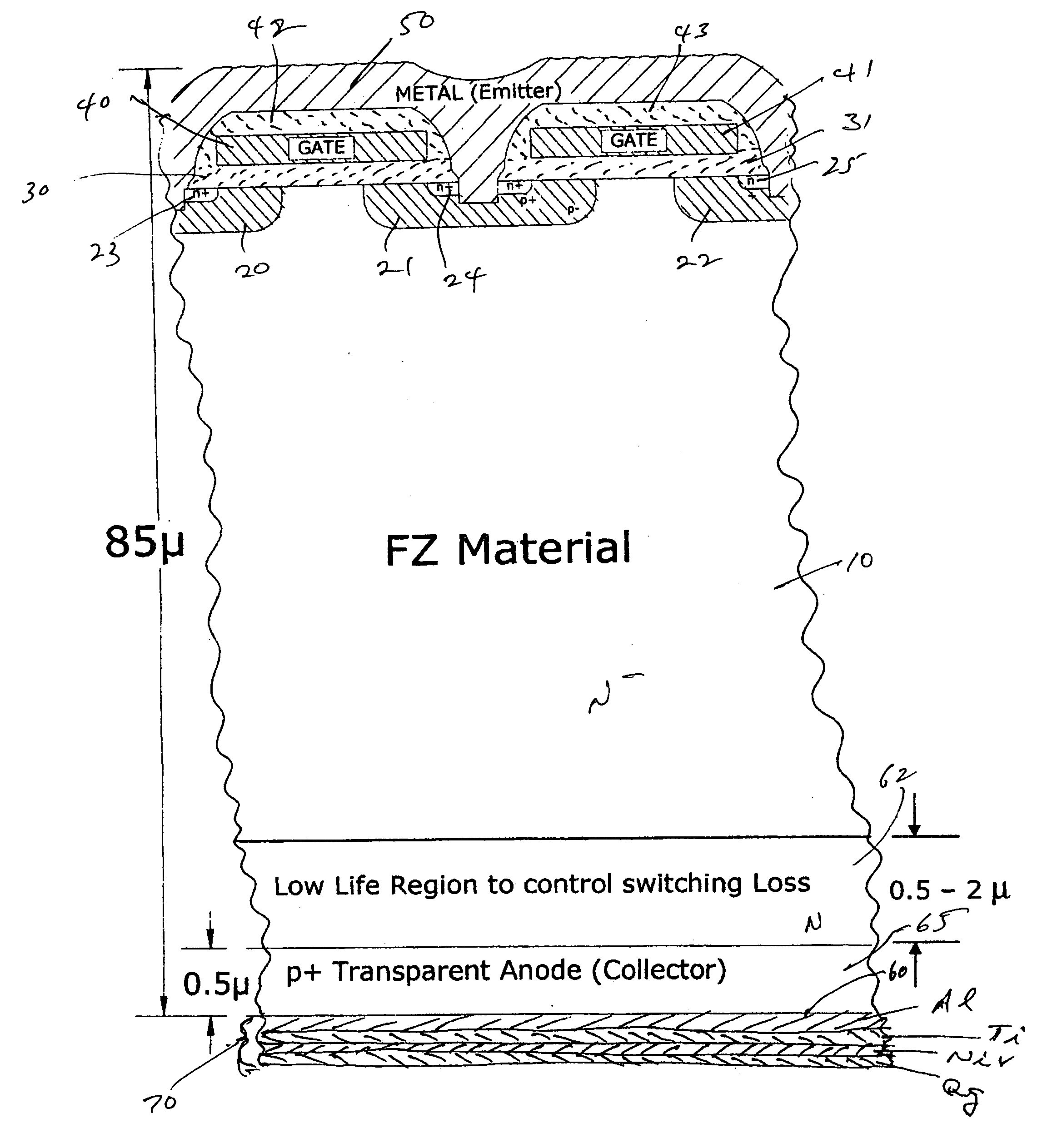
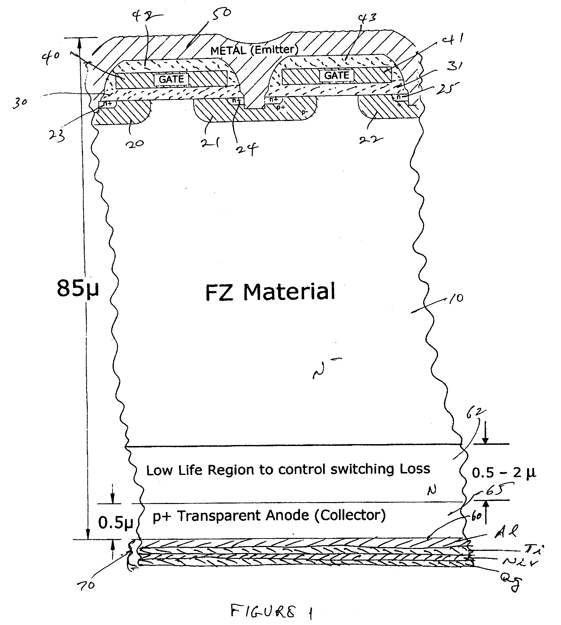
[0016] Returning to FIG. 1, and, in accordance with the invention a light species implant, preferably hydrogen with an energy of 100 to 1000KeV and dose of 1E10 to 1E13 is applied to bottom surface 60 to form damaged low lifetime region 62 to a depth of from 1.0 to 2.5 microns. Thereafter, a P+ transparent anode (or collector) region 65 is formed by implanting a P type dopant, preferably boron, with an energy of 40 to 100 KeV and dose of 1E12 to 1E15 into the backside 60 of wafer 10 to a depth of about 0.5 microns.

[0017] Thereafter, a collector contact 70 is formed by sequentially sputtering metal layers of Al / Ti / NiV / Ag on the backside of wafer 10. Other metals can be used, as desired. The metal sputtering (or other deposition process) is followed by a 30 to 60 minute anneal at 200° C. to 400° C. This anneal process will remove excessive damage caused by the first hydrogen or other light atomic species implant, and enhances the interaction of the aluminum in contact 70 with the sili...

second embodiment

[0018] In the invention, and following the formation of region 65, the wafer 10 is transferred to a backside metal deposition tool and is preheated to 300° C. to 400° C. for 30 to 60 seconds under high vacuum. This is followed by the metal sputtering and anneal of contact 70 as described above. The preheating step under vacuum is useful to remove excess damage caused by the first implant and prepares the silicon surface 60 for strong Al, Si and P type dopant interaction which is critical for anode 65 creation.

[0019] The use of the novel processes described above allows the introduction of low lifetime region 62 in the N− wafer 10 and permits the novel control of the VCEON versus switching energy trade-off by varying the two implant doses, their energy and the anneal temperature, and makes it possible to produce an NPT IGBT well adapted to use in a switch node power supply.


PUM


Abstract

A process for forming an NPT IGBT in a thin N type silicon wafer in which the bottom surface of a thin silicon wafer (100 microns thick or less) has a shallow reduced lifetime region in its bottom formed by a light species atom implant to a depth of less than about 2.5 microns. A P+ transparent collector region about 0.5 microns deep is formed in the bottom of the damaged region by a boron implant. A collector contact of Al/Ti/NiV and Ag is sputtered onto the collector region and is annealed at 200° C. to 400° C. for 30 to 60 minutes. A pre-anneal step before applying the collector metal can be carried out in vacuum at 300° C. to 400° C. for 30 to 60 seconds.

Description

FIELD OF THE INVENTION [0001] This invention relates to Insulated Gate Bipolar Transistors (IGBTs) and more specifically to an IGBT structure and manufacturing process for application to switch mode power supplies (SMPSs). BACKGROUND OF THE INVENTION [0002] IGBTs are well known. IGBTs can be designed for punch through or non-punch through operation. A known IGBT structure and process for its manufacture for IGBTs used for motor control application employ a non-punch through (NPT) mode of operation in which the device is designed to have a low forward voltage drop (VCEON) when the device is conducting, at the expense of an increased turn off energy (EOFF). [0003] Such devices are not well adapted to application to switch mode power supplies in which the turn off energy EOFF is to be minimized, even at the expense of a higher VCEON. [0004] It would be very desirable to provide a process to produce high voltage (eg. 600 volts) NPT IGBTs with a reduced EOFF which do not require substant...

Claims


Application Information

Patent Timeline
Patent Type & Authority Applications(United States)
IPC IPC(8): H01L21/332
CPCH01L29/0834H01L29/41725Y10S438/904H01L29/7395H01L29/66333
Inventor FRANCIS, RICHARDNG, CHIU
Owner INFINEON TECH AMERICAS CORP
Why Eureka
Try Eureka