Method for forming polycrystalline silicon thin film

a technology of polycrystalline silicon and thin film, which is applied in the direction of vacuum evaporation coating, coating, sputtering coating, etc., can solve the problems of high expansion coefficient of plastic substrate, low melting point of plastic substrate, and inability to meet high-temperature manufacturing of polysilicon-based devices, so as to increase the reliability and life of polysilicon-based devices

Inactive Publication Date: 2007-02-01
IND TECH RES INST
View PDF5 Cites 4 Cited by
  • Summary
  • Abstract
  • Description
  • Claims
  • Application Information

AI Technical Summary

Benefits of technology

[0008] It is a primary object of the present invention to provide a method for forming a polycrystalline silicon thin film, using a metal or magnetic substrate so as to increase the reliability and lifetime of the polysilicon-based device.

Problems solved by technology

However, the plastic substrate suffers from its low melting point and is thus not suitable for high-temperature manufacturing of polysilicon-based devices.
On the other hand, the thermal expansion coefficient of the plastic substrate is much larger than that of the glass substrate, and therefore problems due to interface stress may damage the devices.
Moreover, the plastic substrate often generates statistic charges when being rubbed, which causes reduction of the lifetime and reliability of the devices.
However, the above-mentioned prior art reference is disadvantageous because the process is complicated and the cost is high.

Method used


Image

  • Method for forming polycrystalline silicon thin film
  • Method for forming polycrystalline silicon thin film
  • Method for forming polycrystalline silicon thin film

Examples


Embodiment Construction

[0018] The present invention providing a method for forming a polycrystalline silicon thin film can be exemplified by the preferred embodiments as described hereinafter.

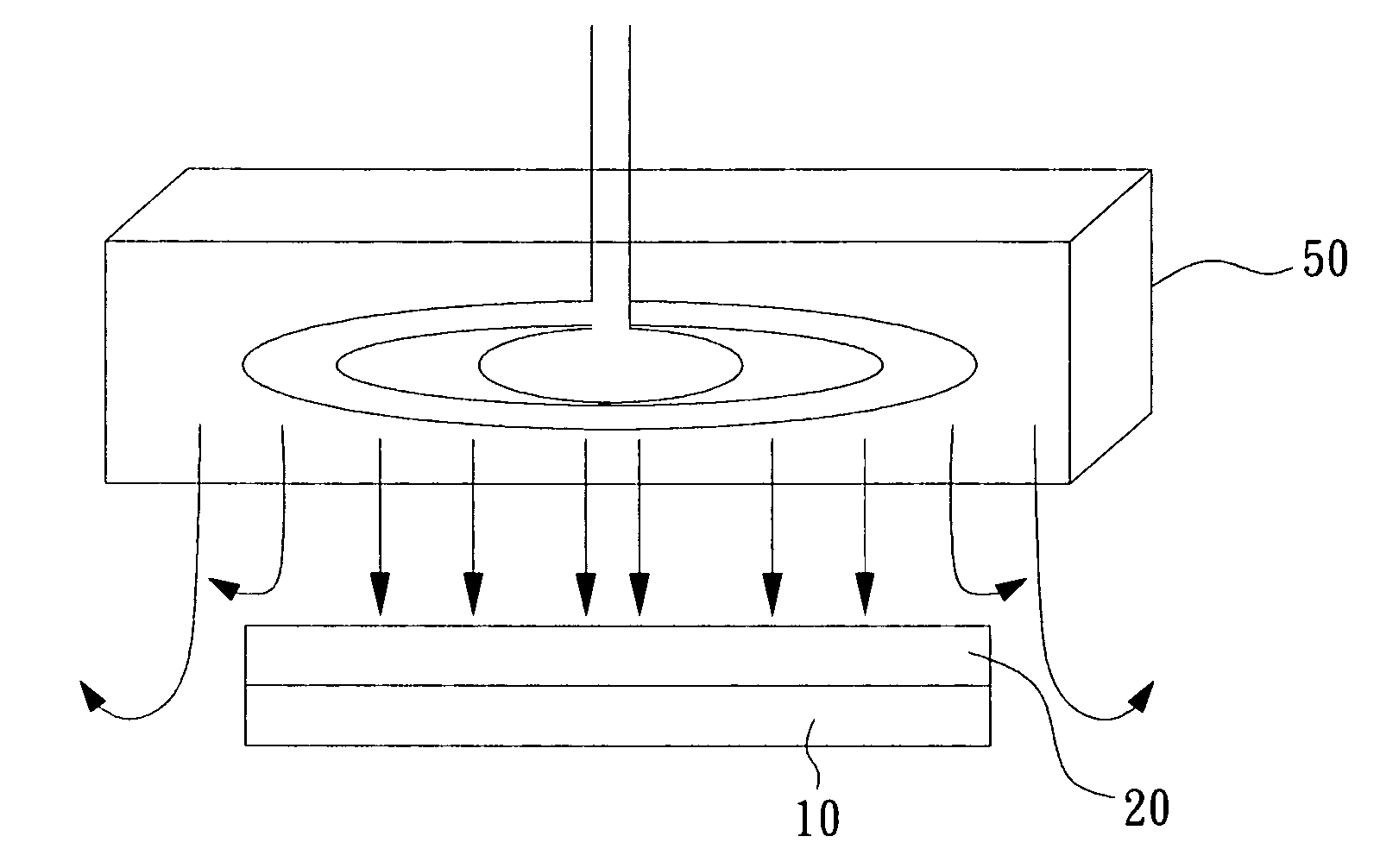
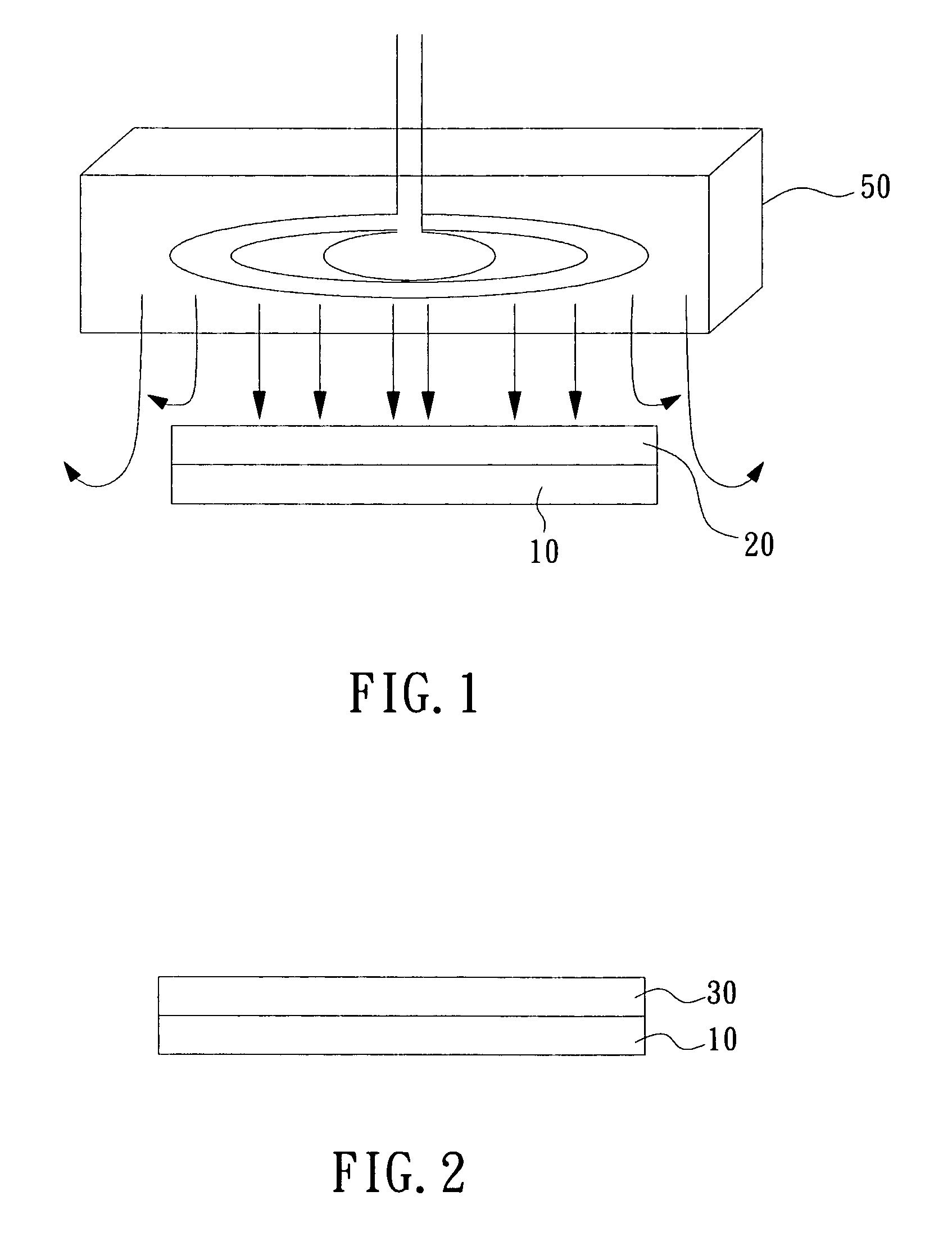
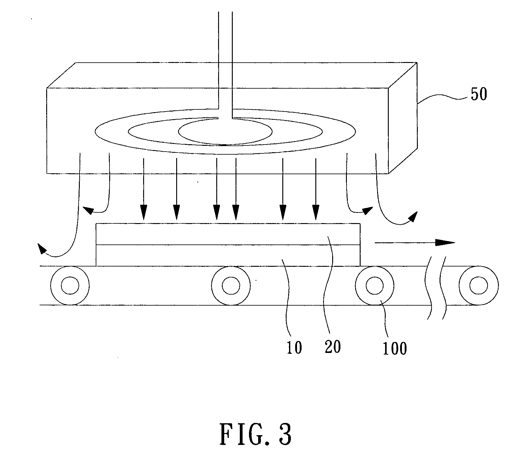
[0019] Please refer to FIG. 1, which is a schematic diagram describing a method for forming a polycrystalline silicon thin film in accordance with the present invention. In FIG. 1, there is provided a substrate 10, on which an amorphous silicon thin film 20 is formed. A heating device 50 is used to heat up the amorphous silicon thin film 20 so as to form a polycrystalline silicon thin film 30 as shown in FIG. 2. Preferably, the heating device 50 is a high-frequency annealing device.

[0020] The substrate 10 is a metal or magnetic substrate. The substrate 10 can also be implemented using a flexible substrate. Preferably, the metal substrate 10 is a stainless steel foil.

[0021] In one preferred embodiment, the high-frequency annealing device 50 comprises a radio frequency (RF) generator so as to perform high-frequency ...


PUM

PropertyMeasurementUnit
flexibleaaaaaaaaaa
magneticaaaaaaaaaa
frequencyaaaaaaaaaa

Abstract

A method for forming a polycrystalline silicon thin film, comprising steps of: providing a substrate; forming an amorphous silicon thin film on the substrate; and inducing a plurality of eddy currents to heat up the substrate such that the amorphous silicon thin-film is annealed to form the polycrystalline silicon thin film.

Description

BACKGROUND OF THE INVENTION [0001] 1. Field of the Invention [0002] The present invention generally relates to a method for forming a polycrystalline silicon thin film and, more particularly, to a method for forming a polycrystalline silicon thin film using high-frequency annealing so as to form the polycrystalline silicon thin film with improved reliability and lowered cost. [0003] 2. Description of the Prior Art [0004] The flexible display has attracted considerable attention in the industry of flat panel displays due to its compactness and portability. It is usually fabricated on a plastic substrate instead of the conventional glass substrate that has been used in liquid crystal displays (LCD's) and organic light emitting diode (OLED). [0005] However, the plastic substrate suffers from its low melting point and is thus not suitable for high-temperature manufacturing of polysilicon-based devices. On the other hand, the thermal expansion coefficient of the plastic substrate is much...

Claims


Application Information

Patent Timeline
Patent Type & Authority Applications(United States)
IPC IPC(8): H01L21/20H01L21/36
CPCC23C14/16H01L21/2022C23C14/5806H01L21/02667H01L21/02425H01L21/02532
Inventor CHANG, CHI-MINGCHANG, JUNG-FANGCHEN, HUNG-TSEWONG, TE-CHI
Owner IND TECH RES INST
Why Eureka
Try Eureka