Resource estimation for design planning

a technology of resource estimation and design planning, applied in the direction of cad circuit design, program control, instruments, etc., can solve the problems of complex designs that are suitable candidates for use with platform (or structured) application specific integrated circuits (platform asics), design cannot fit the selected platform, device or slice, and can suffer a major set-back

Inactive Publication Date: 2007-02-01
BELL SEMICON LLC
View PDF18 Cites 16 Cited by
  • Summary
  • Abstract
  • Description
  • Claims
  • Application Information

AI Technical Summary

Benefits of technology

[0010] The objects, features and advantages of the present invention include providing a method for resource estimation during design planning that may (i) automatically generate estimated RTL or gate representations based upon a user's high-level estimations, (ii) provide estimated RTL or gate representations havi

Problems solved by technology

When the design planning tasks are not performed early or the design planning tasks are not estimated correctly, a project can suffer a major set-back.
Complex designs that are suitable candidates for use with platform (or structured) application specific integrated circuits (platform ASICS) can be incomplete when a customer needs to make design decisions (e.g., select the platform, device or slice), calculate cost and margin based on the slice selected, etc.).
Serious problems can arise when, later in the design process, the customer finds that the design does not fit the selected platform, device or slice.
Accurately estimating the requirements of a design can be difficult for customers, especially less experienced ones.
With the second method, a more accurate estimation can be made, but the estimation is still subject to accuracy problems.
The first solution is undesirable because of the reliance on the expertise of the engineer.
The engineer can e

Method used


Image

  • Resource estimation for design planning
  • Resource estimation for design planning
  • Resource estimation for design planning

Examples


Embodiment Construction

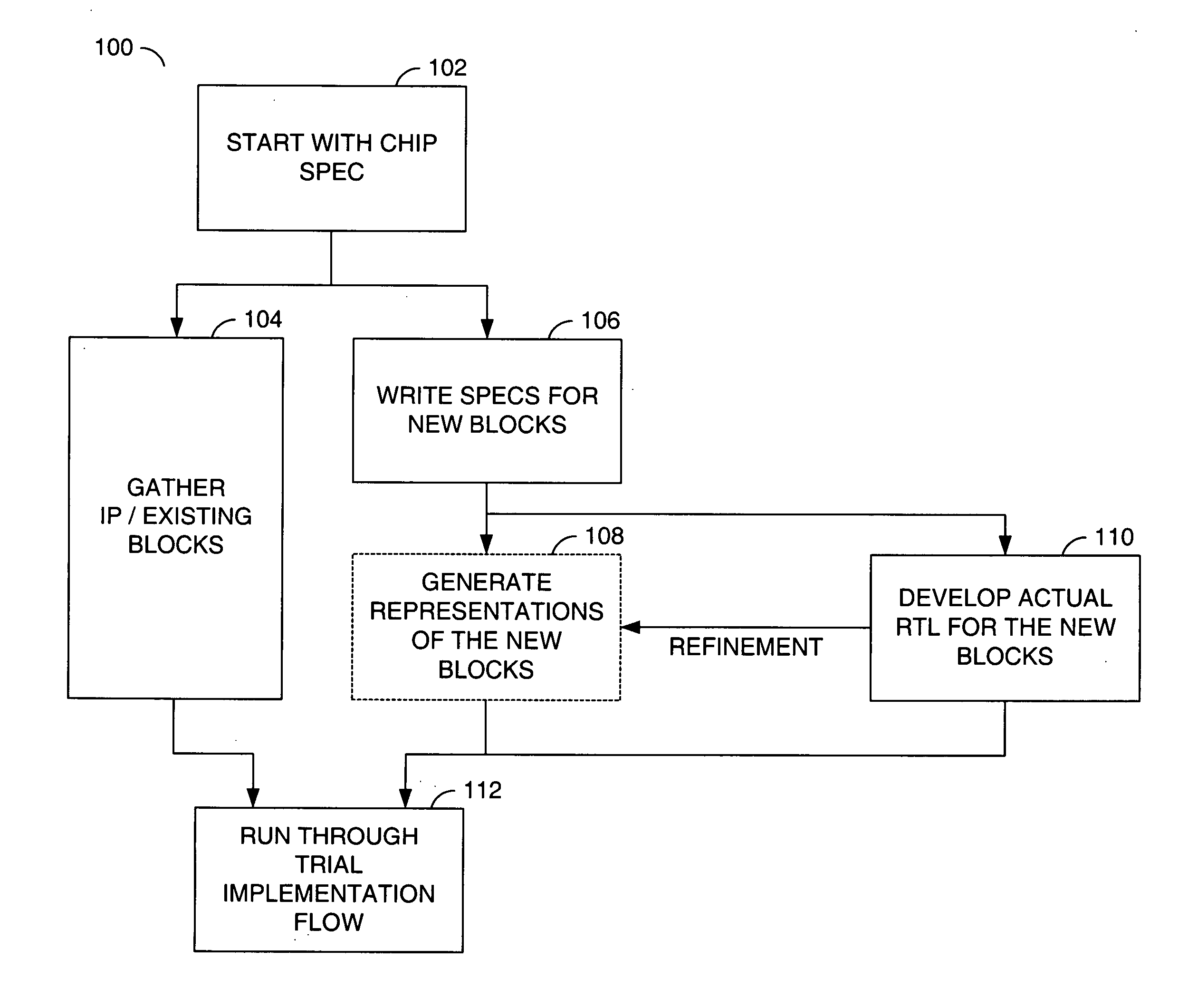
[0014] Referring to FIG. 1, a block diagram is shown illustrating a portion of a design planning flow 100 in accordance with a preferred embodiment of the present invention. The design planning flow 100 may comprise a block (or step) 102, a block (or step) 104, a block (or step) 106, a block (or step) 108, a block (or step) 110 and a block (or step) 112. The block 102 may comprise an integrated circuit (or chip) design specification gathering step. The block 104 may comprise an intellectual property (IP) / existing block gathering step. The block 106 may comprise a new block specification writing step. The block 108 may comprise a representative (or dummy) block generating step. The block 110 may comprise a development step for generating real register transfer level (RTL) representations of the new blocks. The block 112 may comprise a trial implementation flow step.

[0015] In the block 102, specifications for an integrated circuit (or chip) design may be gathered. In the block 104, i...


PUM


Abstract

A method for estimating resources during design planning is generally provided. A first step generally involves receiving design information for an integrated circuit design. A first portion of the integrated circuit design is generally complete, while a second portion of the integrated circuit design is generally incomplete. A second step generally involves receiving user input of estimated design information for the second portion of the integrated circuit design. A third step generally involves automatically generating one or more representative blocks representing the second portion of the integrated circuit design based on the user input. The one or more representative blocks may be generated having substantially equivalent size and characteristics to one or more actual blocks developed for the second portion of the integrated circuit design.

Description

FIELD OF THE INVENTION [0001] The present invention relates to integrated circuit design planning generally and, more particularly, to resource estimation for design planning. BACKGROUND OF THE INVENTION [0002] Frequently, design planning (e.g., die size / device selection, layout analysis, power estimation, etc.) is performed early in a design cycle. Because the design planning can be performed a long time before the actual design is complete (i.e., RTL finished), design planning tasks are often performed with “rules of thumb” based on experience of the designer. When the design planning tasks are not performed early or the design planning tasks are not estimated correctly, a project can suffer a major set-back. For example, a project can be set-back when design analysis assumptions (i.e., ability to fit a design into a particular programmable platform device) are incorrect. [0003] Complex designs that are suitable candidates for use with platform (or structured) application specific...

Claims


Application Information

Patent Timeline
IPC IPC(8): G06F17/50
CPCG06F17/5045G06F30/30
Inventor MARTIN, GREGOR J.LINDBERG, GRANTHE, YING CHUN
Owner BELL SEMICON LLC
Why Eureka
Try Eureka