Pre-made cleavable substrate method and structure of fabricating devices using one or more films provided by a layer transfer process

a technology of layer transfer and substrate, which is applied in the direction of semiconductor devices, electrical appliances, adhesives, etc., can solve the problems of brittle materials, difficult to separate or cut extremely hard materials, and often difficult to achieve the separation or cutting of extremely hard materials. , to achieve the effect of preventing the possibility of damage to the film or a remaining portion of the substrate and facilitating processing

Inactive Publication Date: 2007-02-08
SILICON GENERAL CORPORATION
View PDF85 Cites 44 Cited by
  • Summary
  • Abstract
  • Description
  • Claims
  • Application Information

AI Technical Summary

Benefits of technology

[0016] Numerous benefits are achieved over pre-existing techniques using the present invention. In particular, the present invention uses controlled energy and selected conditions to preferentially cleave a thin film of material without a possibility of damage to such film from excessive energy release. This cleaving process selectively removes the thin film of material from the substrate while preventing a possibility of damage to the film or a remaining portion of the substrate. Additionally, the present method and structures allow for more efficient processing using a cleave layer provided in a substrate through the course of semiconductor processing, which may occur at higher temperatures, according to a specific embodiment Once the cleaved layer has been subjected to integrated circuit processing techniques, a handle substrate, which held the cleaved layer is debondable. In a preferred embodiment, the present invention provides a multi-layered substrate that can withstand semiconductor processing but still allow for a thin layer to be debondable in an efficient manner without damaging the thin layer including any of the devices thereon. Depending upon the embodiment, one or more of these benefits may be achieved. These and other benefits may be described throughout the present specification and more particularly below.

Problems solved by technology

This technique, however, is often extremely “rough” and cannot generally be used for providing precision separations in the substrate for the manufacture of fine tools and assemblies.
Additionally, the saw operation often has difficulty separating or cutting extremely hard and or brittle materials, such as diamond or glass.
The saw operation also cannot be used effectively for the manufacture of microelectronic devices, including integrated circuit devices, and the like.
Making devices smaller is very challenging, as each process used in integrated fabrication has a limit.
Additionally, as devices require faster and faster designs, process limitations exist with certain conventional processes and materials.
A conventional process often used to thin these device layers is often called “back grinding,” which is often cumbersome, prone to cause device failures, and can only thin the device layer to a certain thickness.
Although there have been significant improvements, such back grinding processes still have many limitations.

Method used


Image

  • Pre-made cleavable substrate method and structure of fabricating devices using one or more films provided by a layer transfer process
  • Pre-made cleavable substrate method and structure of fabricating devices using one or more films provided by a layer transfer process
  • Pre-made cleavable substrate method and structure of fabricating devices using one or more films provided by a layer transfer process

Examples


Embodiment Construction

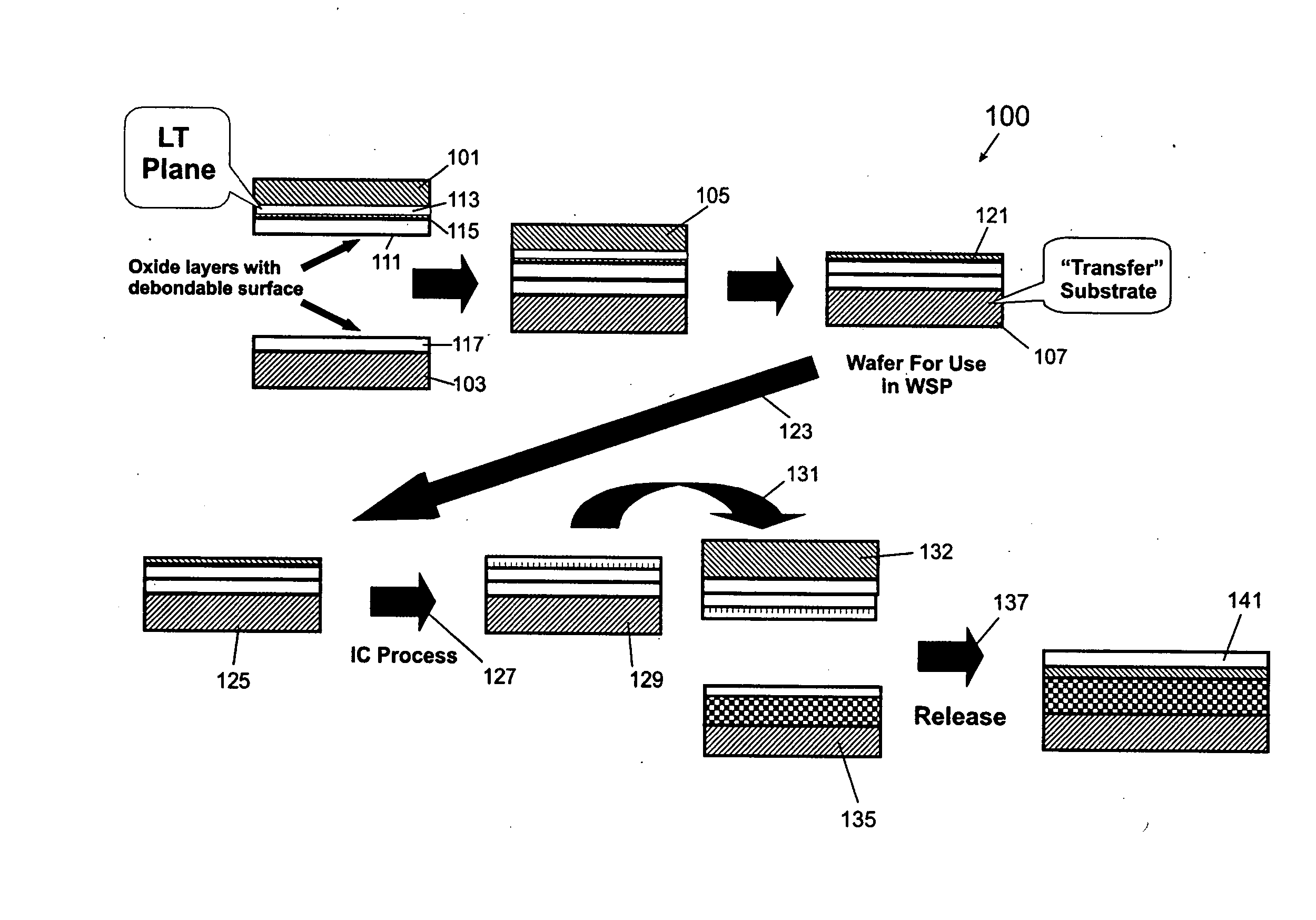
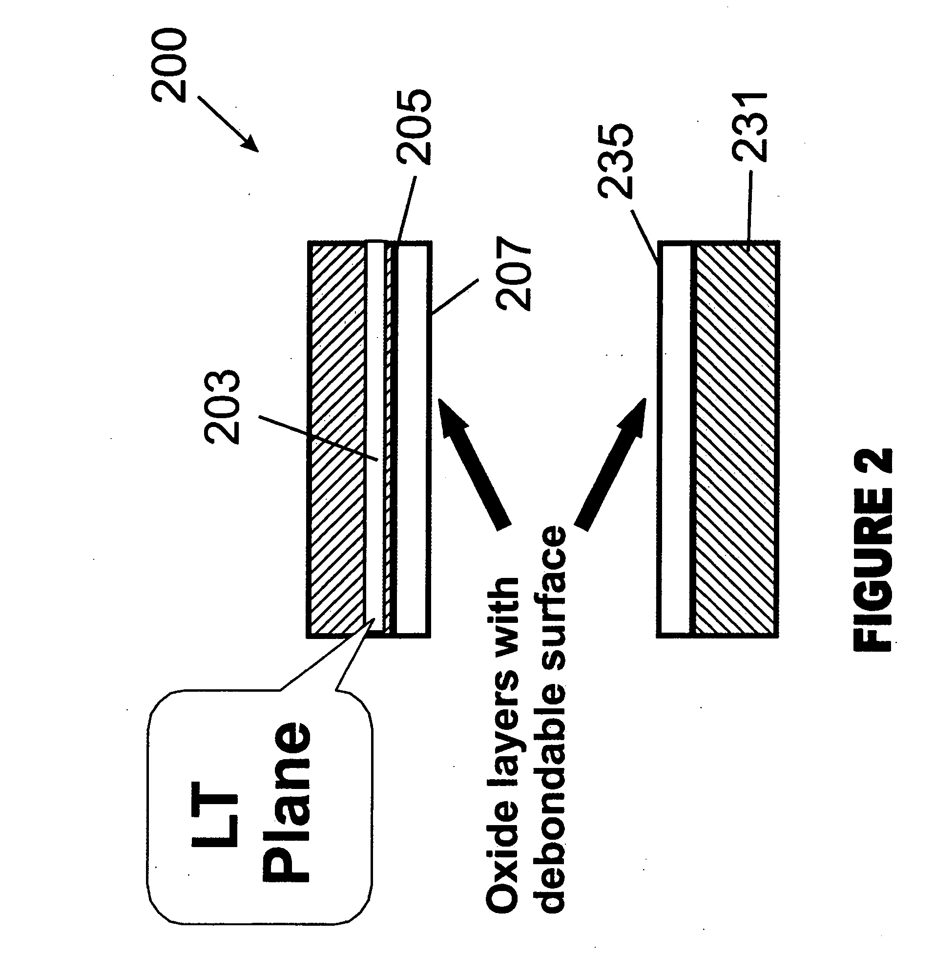
[0020] According to the present invention, techniques related to the manufacture of substrates are provided. More particularly, the invention provides a technique including a method and a structure for forming multi-layered substrate structures for the fabrication of substrates for semiconductor integrated circuit devices using layer transfer techniques. But it will be recognized that the invention has a wider range of applicability; it can also be applied to other types of substrates for three-dimensional packaging (e.g., wafer scale) of integrated semiconductor devices, photonic devices, piezoelectronic devices, flat panel displays, microelectromechanical systems (“MEMS”), nano-technology structures, sensors, actuators, solar cells, biological and biomedical devices, and the like.

[0021] Referring to FIG. 1, a method 100 for fabricating integrated circuits on a layer transferred substrate according to embodiments of the present invention may be outlined as follows:

[0022] 1 Provid...


PUM

PropertyMeasurementUnit
temperatureaaaaaaaaaa
surface roughnessaaaaaaaaaa
temperatureaaaaaaaaaa

Abstract

A method for fabricating one or more devices, e.g., integrated circuits. The method includes providing a multi-layered substrate, which has a thickness of material (e.g., single crystal silicon) overlying a first debondable surface coupled to and overlying a second debondable surface. The second debondable surface is overlying an interface region of the multi-layered substrate. In a preferred embodiment, the thickness of material having a surface region. The method includes processing the surface region of the multi-layered substrate using one or more processes to form at least one device onto a portion of the surface region. The method includes forming a planarized upper surface region overlying the surface region of the thickness of material. The method includes joining the planarized upper surface region to a face of a handle substrate. In a preferred embodiment, the method includes processing the first debondable surface and the second debondable surface to change a bond strength from a first determined amount to a second determined amount, which is capable of debonding the first debondable surface from the second debondable surface. The method includes debonding the first debondable surface from the second debondable surface to release the thickness of material and the handle substrate.

Description

BACKGROUND OF THE INVENTION [0001] The present invention relates to the manufacture of substrates. More particularly, the invention provides a technique including a method and a structure for forming multi-layered substrate structures for the fabrication of substrates for semiconductor integrated circuit devices using layer transfer techniques. But it will be recognized that the invention has a wider range of applicability; it can also be applied to other types of substrates for three-dimensional packaging of integrated semiconductor devices, photonic devices, piezoelectronic devices, flat panel displays, microelectromechanical systems (“MEMS”), nano-technology structures, sensors, actuators, solar cells, biological and biomedical devices, and the like. [0002] From the very early days, human beings have been building useful articles, tools, or devices using less useful materials for numerous years. In some cases, articles are assembled by way of smaller elements or building blocks. ...

Claims


Application Information

Patent Timeline
Patent Type & Authority Applications(United States)
IPC IPC(8): B29C63/00
CPCB29C63/0013H01L21/6835Y10T156/1184Y10T156/11H01L2221/68368
Inventor HENLEY, FRANCOIS J.
Owner SILICON GENERAL CORPORATION
Why Eureka
Try Eureka