

Power plane design and jumper wire bond for voltage drop minimization
a technology of voltage drop and jumper wire, which is applied in the direction of semiconductor devices, semiconductor/solid-state device details, electrical apparatus, etc., can solve the problems of voltage or ir drop, undesirable “hot spots", and negatively affecting the performance of circuitry
- Summary
- Abstract
- Description
- Claims
- Application Information
AI Technical Summary
Benefits of technology
Problems solved by technology
Method used
Image

Examples
Embodiment Construction
[0012] It should be understood at the outset that although example embodiments of the present invention are illustrated below, the present invention may be implemented using any number of techniques, whether currently known or in existence. The present invention should in no way be limited to the example embodiments, drawings, and techniques illustrated below, including the embodiments and implementation illustrated and described herein. Additionally, the drawings are not necessarily drawn to scale.
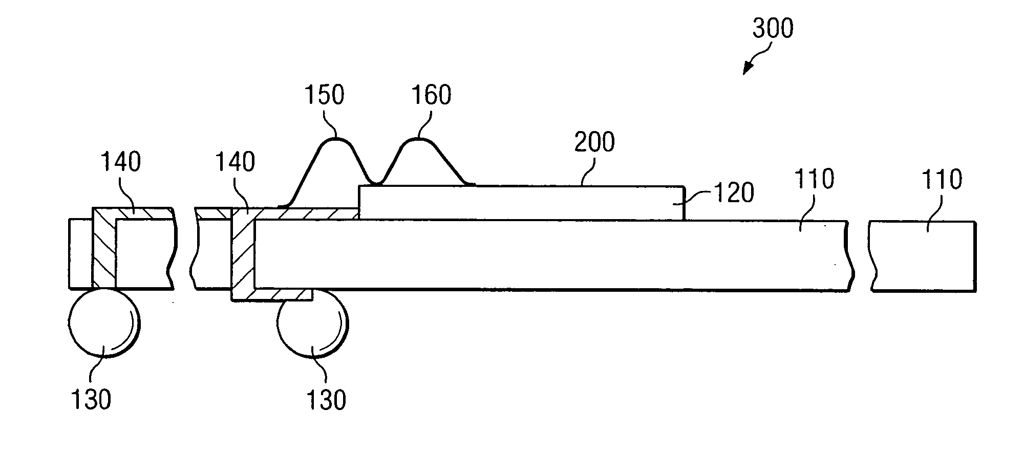
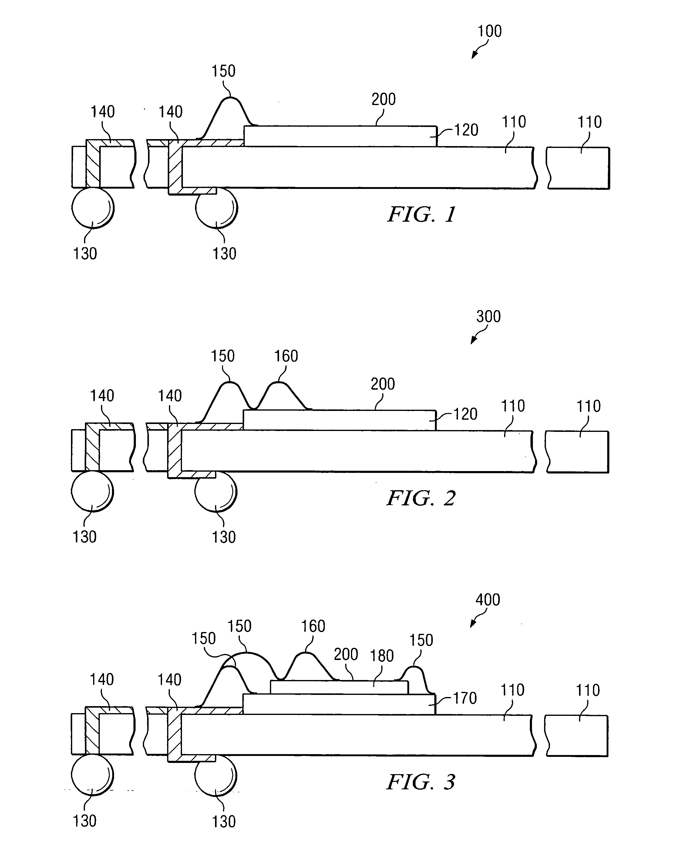
[0013]FIG. 1 shows a side-cross sectional view of a conventional power system 100. The conventional power system 100 include solder balls 130, traces 140, and a wire bond connection 150. With the conventional power system 100, electrical current or power may be communicated to a die 120 by traveling from the solder balls 130 (e.g., ball-grid array balls) through the traces 140 and the wire bond connections 150 to a surface perimeter of the die 120, for example, a pad (not explicitly show...
PUM
 Abstract
Description
Claims
Application Information