Electron emission device

a technology of emission device and emission tube, which is applied in the direction of discharge tube/lamp details, single discharge path tube, gas-filled discharge tube, etc., can solve the problems of low discharge efficiency, difficulty in employing field emission method, and energy for heating

Inactive Publication Date: 2007-02-08
KK TOSHIBA
View PDF7 Cites 4 Cited by
  • Summary
  • Abstract
  • Description
  • Claims
  • Application Information

AI Technical Summary

Problems solved by technology

However, in case of heating, the energy for heating is required and switching on and off of discharge cannot be performed promptly, because a change in temperature requires time.
As a result, the operations accompany indistinctness in control, which is a serious problem from a practical point of view.
However, it is difficult to employ the field emission method in cases where stable electron emission is required over a long period of time or electron emission is greatly affected by the variation in emission current, because the discharge characteristics vary due to adhesion of ionized elements or the likes.
However, there is the problem of low discharge efficiency, as the number of electrons to be emitted is small for the voltage to be applied to excite every electrons to such a degree as to cause electron emission.
However, it is difficult to emit primary electrons uniformly and evenly to the diamond barrier, as the primary electrons have energizes to emit secondary electrons.

Method used


Image

  • Electron emission device
  • Electron emission device
  • Electron emission device

Examples


first embodiment

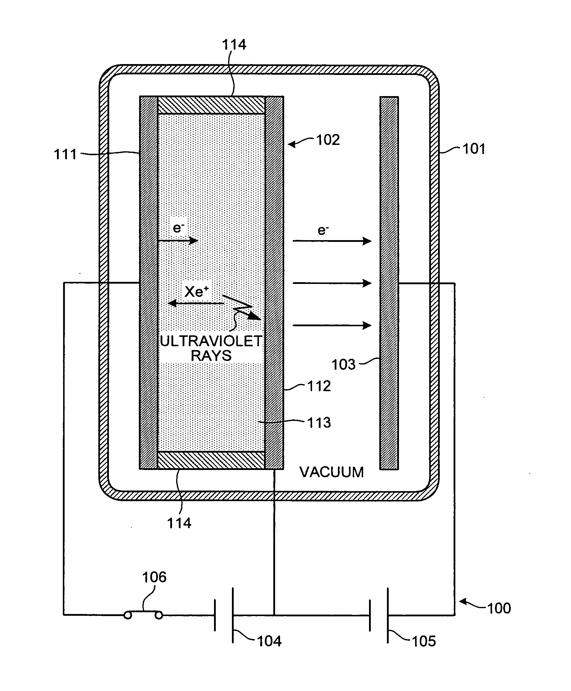
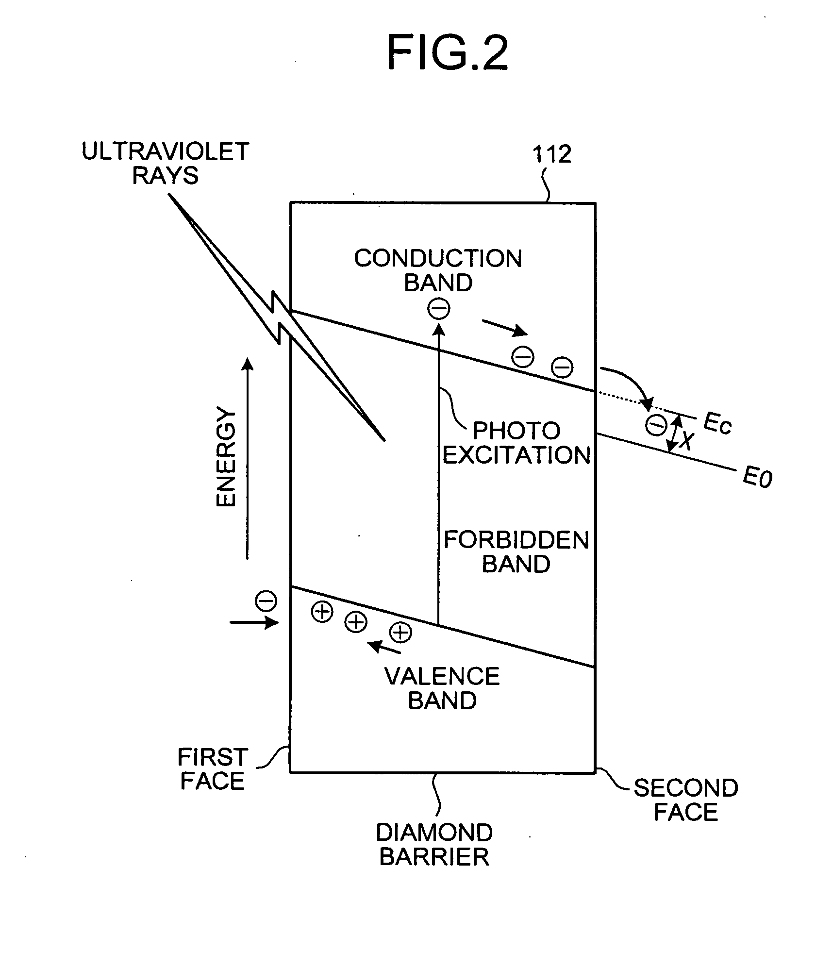
[0024]FIG. 1 is a side cross-sectional view showing an electron emission device 100 in accordance with the present invention. As shown in this drawing, the electron emission device 100 has a discharge cell 102 and a discharge anode 103 provided inside an airtight container 101 to be evacuated, and also has a turn-off switch 106, a first power source 104 and a second power source 105 provided outside the airtight container 101. Since this drawing was prepared for ease of explanation, the size ratio of this draining is not necessarily the same as those in the explanation and the other drawings.

[0025] The airtight container 101 is evacuated so as to discharge electrons in a vacuum. The airtight container 101 may have any shape and size, and may be made of any kind of material, as long as it can be evacuated. In a case where a fluorescent material is applied to the discharge anode 103, for example, the discharged electrons run into the fluorescent material to generate light. In that cas...

third embodiment

[0061] The above described electron emission device of this embodiment can only control the switching on and off of electron emission by the turn-off switch 106, so as to adjust the amount of electrons to be emitted. However, the present invention is not limited to such a control operation, and a mechanism for controlling the amount of current or the amount of electrons to be emitted may be employed. Therefore, a structure that further includes a variable resistor so as to control the amount of electrons to be emitted is provided as a

[0062]FIG. 7 is a side cross-sectional view showing an electron emission device 700 in accordance with a third embodiment. The electron emission device 700 differs from the electron emission device 500 of the second embodiment in further including a variable resistor 701 and having a turn-off switch 702 located in a different position from the turn-off switch 106. In the following description, the same components as those of the first and second embodim...


PUM


Abstract

The electron emission device includes a first electrode; a semiconductor barrier that has a first face disposed to face the first electrode and a second face which is opposite face of the first face, and is formed with a wide bandgap semiconductor; an insulating material that forms a space sealed between the first electrode and the semiconductor barrier; an inert gas that is encapsulated in the space; a second electrode that is disposed to face a second face of the semiconductor barrier interposing vacuum therebetween; a first voltage applying unit that applies a voltage between the first electrode and the semiconductor barrier; and a second voltage applying unit that applies a voltage between the semiconductor barrier and the second electrode.

Description

CROSS-REFERENCE TO RELATED APPLICATIONS [0001] This application is based upon and claims the benefit of priority from the prior Japanese Patent Application No. 2005-225898, filed on Aug. 3, 2005; the entire contents of which are incorporated herein by reference. BACKGROUND OF THE INVENTION [0002] 1. Field of the Invention [0003] The present invention relates to an electron emission device that emits electrons into a vacuum and a technique of emitting electrons from a plane-type structure upon application of a voltage. [0004] 2. Description of the Related Art [0005] Conventionally, vacuum electron sources that emit electrons into a vacuum have been used as components for various electronic devices. Since the vacuum electron emission sources is an essential element in various devices, there have been a number of studies and developments made for higher performances. [0006] Principles themselves of the electron emission can be roughly divided into the following categories: a thermal el...

Claims


Application Information

Patent Timeline
Patent Type & Authority Applications(United States)
IPC IPC(8): H01J17/02
CPCH01J21/04H01J3/021
Inventor SAKAI, TADASHIONO, TOMIOSAKUMA, NAOSHIYOSHIDA, HIROAKISUZUKI, MARIKO
Owner KK TOSHIBA
Why Eureka
Try Eureka