Device selection circuitry constructed with nanotube technology

a technology of nanotubes and devices, applied in nanoelectromechanical switches, nanoinformatics, instruments, etc., can solve the problems of long write cycles (ms), low relative speed of dram or sram, and relatively low cost of rom,

Inactive Publication Date: 2007-02-08
NANTERO
View PDF4 Cites 244 Cited by
  • Summary
  • Abstract
  • Description
  • Claims
  • Application Information

AI Technical Summary

Problems solved by technology

ROM is relatively low cost but cannot be rewritten.
EEPROM (or “Flash”) is inexpensive, and has low power consumption but has long write cycles (ms) and low relative speed in comparison to DRAM or SRAM.
Flash also has a finite number of read / write cycles leading to low long-term reliability.
SRAM does not need to be refreshed and is fast relative to DRAM, but has lower density and is more expensive relative to DRAM.
Both SRAM and DRAM are volatile, meaning that if power to the memory is interrupted the memory will lose the information stored in the memory cells.
Consequently, existing technologies are either non-volatile but are not randomly accessible and have low density, high cost, and limited ability to allow multiples writes with high reliability of the circuit's function, or they are volatile and complicate system design or have low density.
A different memory cell based upon magnetic tunnel junctions has also been examined but has not led to large-scale commercialized MRAM devices.
FRAM suffers from a large memory cell size, and it is difficult to manufacture as a large-scale integrated component.
While the nonvolatility condition is met, this technology appears to suffer from slow operations, difficulty of manufacture and reliability and has not reached a state of commercialization.
This form of memory requires highly specialized wire junctions and may not retain non-volatility owing to the inherent instability found in redox processes.
These techniques are now believed to be difficult to employ at commercial scales using modern technology.
Moreover, they may contain inherent limitations such as the length of the nanotubes that may be grown reliably using these techniques, and it may difficult to control the statistical variance of geometries of nanotube wires so grown.

Method used


Image

  • Device selection circuitry constructed with nanotube technology
  • Device selection circuitry constructed with nanotube technology
  • Device selection circuitry constructed with nanotube technology

Examples


Embodiment Construction

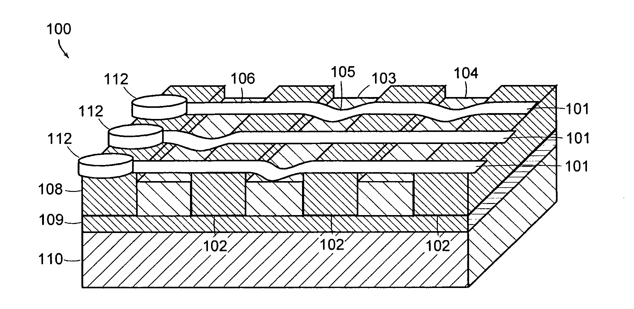
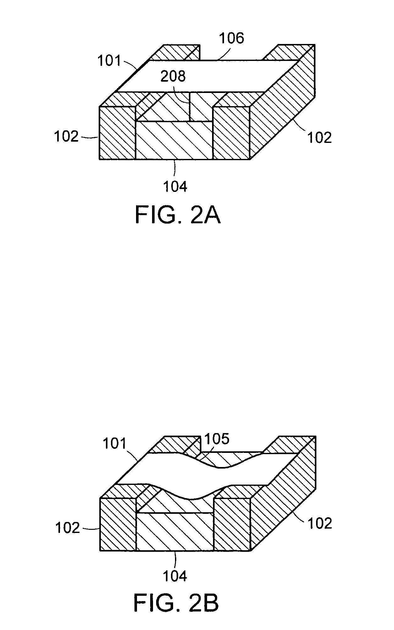
[0027] Preferred embodiments of the invention provide new electromechanical memory arrays and methods for making same. In particular, electromechanical memory cells are created that operate anaologously to the NTWCM devices disclosed in WO 01 / 03208, which is hereby incorporated by reference in its entirety. However, unlike the NTWCM devices disclosed in WO01 / 03208, preferred embodiments of the invention replace the suspended nanoscopic wires used in the NTWCM devices with new ribbons made from a matted layer of nanotubes or a non-woven fabric of nanotubes. These new devices are referred to herein as nanotube ribbon crossbar memories (NTRCMs). The new nanotube belt structures are believed to be easier to build at the desired levels of integration and scale (in number of devices made) and the geometries are more easily controlled.

[0028] Because the new nanotube belt crossbar memory devices operate analogously to NTWCM, the description of their architecture and principles of operation...


PUM


Abstract

A memory system having electromechanical memory cells and decoders is disclosed. A decoder circuit selects at least one of the memory cells of an array of such cells. Each cell in the array is a crossbar junction at least one element of which is a nanotube or a nanotube ribbon. The decoder circuit is constructed of crossbar junctions at least one element of each junction being a nanotube or a nanotube ribbon.

Description

CROSS-REFERENCE TO RELATED APPLICATIONS [0001] This application is a continuation of and claims priority under 35 U.S.C. § 120 to U.S. patent application Ser. No. 10 / 693,241, filed Oct. 24, 2003 and entitled “Device Selection Circuitry Constructed with Nanotube Technology,” which is a continuation of U.S. patent application Ser. No. 09 / 915,173, now U.S. Pat. No. 6,643,165, filed Jul. 25, 2001 and entitled “Electromechanical Memory Having Cell Selection Circuitry Constructed With Nanotube Technology,” the entire contents of which are incorporated herein by reference, which is related to the following patents, filed Jul. 25, 2001, which are incorporated herein by reference in their entireties: [0002] U.S. Pat. No. 6,574,130, entitled “Hybrid Circuit Having Nanotube Electromechanical Memory”; and [0003] U.S. Pat. No. 6,919,592, entitled “Electromechanical Memory Array Using Nanotube Ribbons and Method for Making Same.”BACKGROUND [0004] 1. Technical Field [0005] This invention relates i...

Claims


Application Information

Patent Timeline
Patent Type & Authority Applications(United States)
IPC IPC(8): G11C11/00B81B3/00G11C13/02G11C23/00H01L21/768H01L27/10H01L27/12H01L27/24
CPCB82Y10/00G11C13/025G11C23/00G11C2213/77G11C2213/81Y10S977/765H01L27/10H01L27/1203Y10S977/742Y10S977/734Y10S977/943H01H1/0094
Inventor SEGAL, BRENT M.BROCK, DARREN K.RUECKES, THOMAS
Owner NANTERO
Why Eureka
Try Eureka