Semiconductor device and method of manufacturing the same

a technology of semiconductor devices and mosfets, which is applied in the direction of semiconductor devices, semiconductor/solid-state device details, electrical apparatus, etc., can solve the problems of affecting the operation of the device, the effect of reducing the breakdown voltage of the device in the depth direction of the device, and the threshold value changing threshold value, etc., to achieve stable threshold value and high speed

Inactive Publication Date: 2007-02-15
KK TOSHIBA
View PDF6 Cites 12 Cited by
  • Summary
  • Abstract
  • Description
  • Claims
  • Application Information

AI Technical Summary

Benefits of technology

[0034] According to the embodiments of the present invention, it is possible to pro

Problems solved by technology

However, to employ the various kinds of structures result in causing some problems such as deceasing a breakdown voltage and changing a threshold value of the MOSFET due to the structure of the l

Method used


Image

  • Semiconductor device and method of manufacturing the same
  • Semiconductor device and method of manufacturing the same
  • Semiconductor device and method of manufacturing the same

Examples


first embodiment

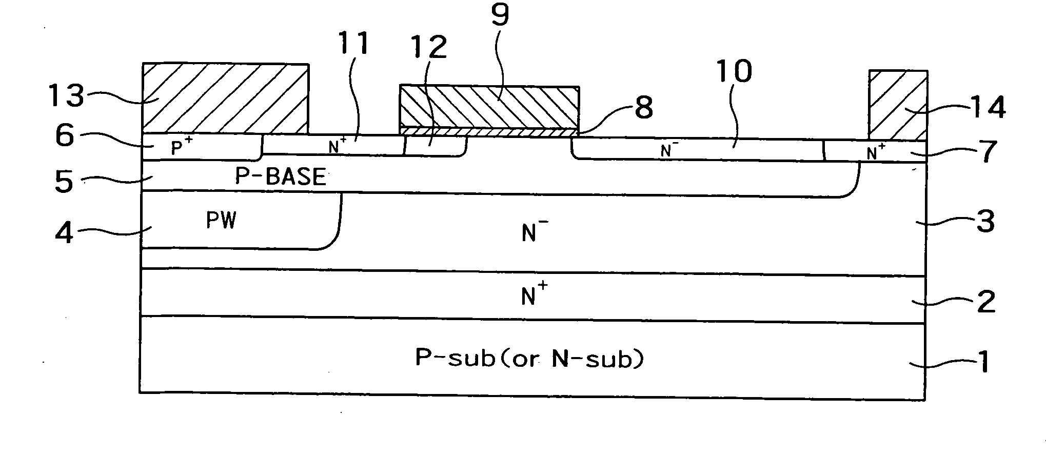
[0048]FIG. 1 is a sectional view of a semiconductor device according to a first embodiment of the present invention.

[0049] As shown in FIG. 1, a semiconductor layer of an n+ type (second conductivity type) serving as a low resistance layer 2 is formed on a substrate 1 of a p type (first conductivity type). Then, a semiconductor layer of an n− type (second conductivity type) serving as a high resistance layer 3 is formed thereon.

[0050] Based on this substrate structure, a p type well 4, a p type base layer 5, an ion or impurity implanted channel region 12, an n− type RESURF layer 10, an n+ type source layer 11, an n+ type drain layer 7, a p+ type layer 6 are selectively formed on the n− type high resistance layer 3.

[0051] The ion implanted channel region 12 of P type is selectively formed in the p type base layer 5, and a gate insulating film 8 and a gate electrode 9 are formed thereon. Next, the n− type RESURF layer 10 is formed at one side of the gate electrode using the gate el...

second embodiment

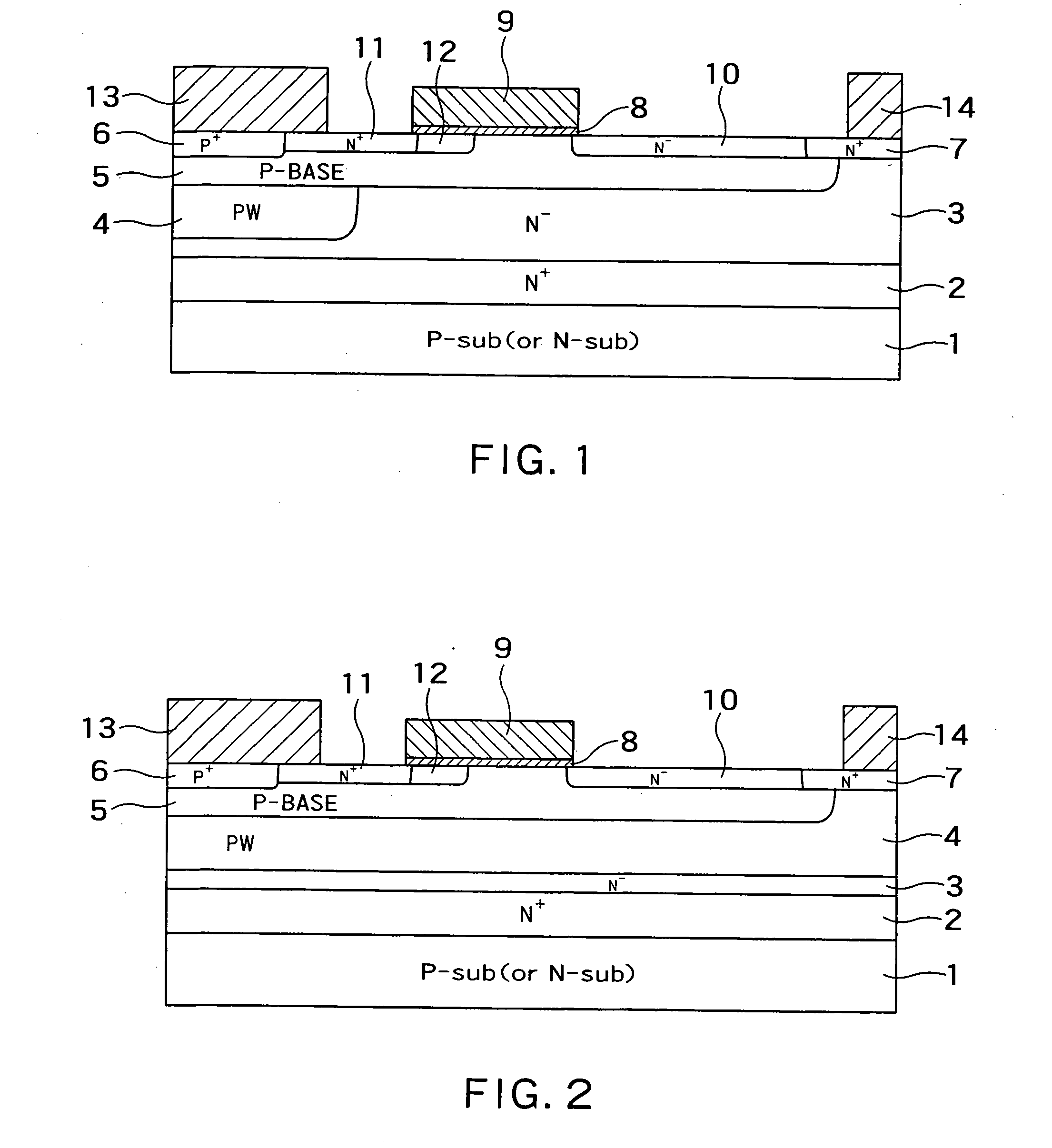
[0059]FIG. 2 is a sectional view of a semiconductor device according to a second embodiment of the present invention.

[0060] As shown in FIG. 2, the second embodiment differs from the first embodiment in that the p type well 4 extends to cover the entire portion of the device. In this case, since the p type well 4 and the source electrode 13 electrically contact each other via the p type base layer 5 and the p+ type layer 6, the device has a potential difference between the source and the drain in a vertical direction at the drain side. Since the p type well layer 4, which is not formed to decide the threshold value, as in the case of this embodiment, generally has a low concentration of 1×10¹⁵−1×1017 cm−3, it is possible to prevent the decrease in breakdown voltage at the PN junction between the n+ type drain layer 7 and the p type well layer 4.

[0061] Accordingly, like the first embodiment, it is possible to obtain a semiconductor device having a stable threshold value and operati...

third embodiment

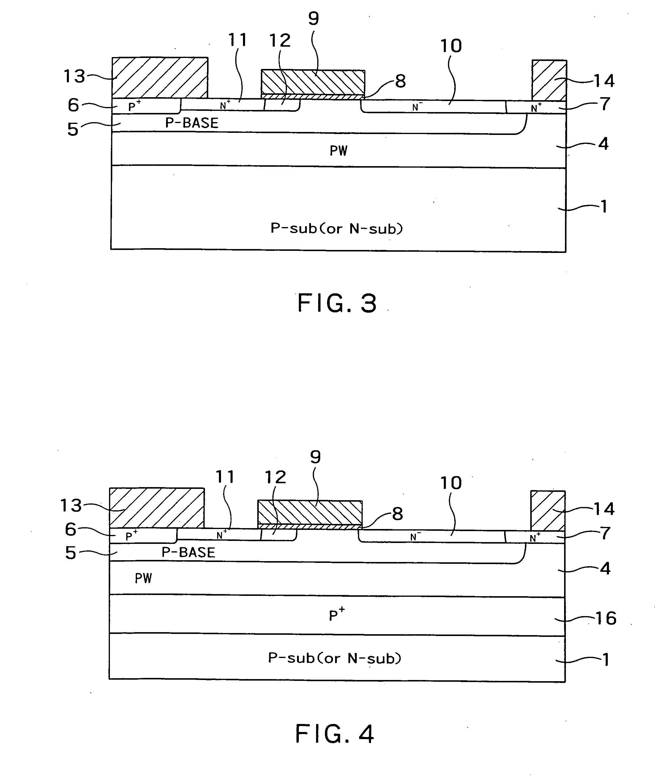
[0062]FIG. 3 is a sectional view of a semiconductor device according to a third embodiment of the present invention.

[0063] As shown in FIG. 3, the third embodiment differs from the second embodiment in that the n+ type embedded layer serving as the low resistance layer 2 and the n− type layer serving as the high resistance layer 3, which are formed on the substrate 1 at the lower portion of the device in an overlapping manner as shown in FIG. 2, are removed.

[0064] As in the case of the second embodiment, the p type well layer 4 extends to cover the entire device in this embodiment. Accordingly, it is possible to decide the device condition by adjusting the potential of the p type well layer 4. Thus, if there is no embedded n+ type layer serving as the low resistance layer 2 and n− type layer serving as the high resistance layer 3 as in the case of the third embodiment, it is possible to obtain the same effect as in the second embodiment.


PUM


Abstract

A semiconductor device comprising: a base layer of a first conductivity type selectively formed above a semiconductor substrate; a gate electrode formed on the base layer via the insulating film; a source layer of a second conductivity type selectively formed at a surface of the base layer at one side of the gate electrode; an channel implantation layer selectively formed at the surface of the base layer so as to be adjacent to the source layer below the gate electrode, the channel implantation layer having a higher concentration than the base layer; a RESURF layer of the second conductivity type selectively formed at the surface of the base layer at the other side of the gate electrode; and a drain layer of a second conductivity type being adjacent to the RESURF layer, a portion of the drain layer overlapping the base layer, and the drain layer having a higher concentration than the RESURF layer.

Description

CROSS-REFERENCE TO RELATED APPLICATION [0001] This application is based upon and claims the benefit of priority from prior Japanese Patent Application No. 2005-233570, filed on Aug. 11, 2005, the entire contents of which are incorporated herein by reference. BACKGROUND OF THE INVENTION [0002] 1. Field of the Invention [0003] The present invention relates to a semiconductor device and a method of manufacturing the same. In particular, the present invention relates to a structure of a lateral MOSFET. [0004] 2. Background Art [0005] There is a lateral MOSFET, as one of the conventional semiconductor devices, that has a middle to high breakdown voltage and operates at a high speed. An example of the structure thereof is as follows. [0006] In a p− type semiconductor substrate, an n+ type source layer and an n+ type drain layer are formed with a predetermined interval. In a region between an n+ type source layer and an n+ type drain layer, as a gate region, a gate electrode is formed via ...

Claims


Application Information

Patent Timeline
IPC IPC(8): H01L23/58
CPCH01L29/7816H01L29/7835H01L29/063H01L29/0878H01L29/1045H01L29/1083H01L2924/0002H01L29/1095H01L29/66681H01L2924/00
Inventor MATSUDAI, TOMOKOYASUHARA, NORIO
Owner KK TOSHIBA
Why Eureka
Try Eureka