Process for manufacturing dual work function metal gates in a microelectronics device

a technology of microelectronic devices and metal gates, which is applied in the direction of basic electric elements, electrical apparatus, and semiconductor devices, can solve the problems of gate charge carriers at the interface between the gate and the gate dielectric, the depletion of gate charge carriers at the interface of the gate and the gate, and the use of doped polysilicon gates

Active Publication Date: 2007-02-15
TEXAS INSTR INC
View PDF3 Cites 419 Cited by
  • Summary
  • Abstract
  • Description
  • Claims
  • Application Information

AI Technical Summary

Problems solved by technology

The use of doped polysilicon gates has become problematic, however, as the dimensions of gates and gate insulators alike have significantly reduced.
This limitation can result in a depletion of gate charge carriers at the interface between the gate and gate dielectric, when the gate is biased to invert the channel.
Consequently, the electrical thickness of the gate stack is substantially increased, thereby deteriorating the performance characteristics of the transistor, such as reducing the drive current and slowing switching speeds.
Depletion of the polysilicon gate is a fundamental issue that limits further scaling of MOS devices.
At present, there is no effective way to control this Vt offset problem.
In the manufacture of microelectronic devices, having independently adjustable dual work function metal gates has been troublesome, however.
However, during fa...

Method used


Image

  • Process for manufacturing dual work function metal gates in a microelectronics device
  • Process for manufacturing dual work function metal gates in a microelectronics device
  • Process for manufacturing dual work function metal gates in a microelectronics device

Examples


Embodiment Construction

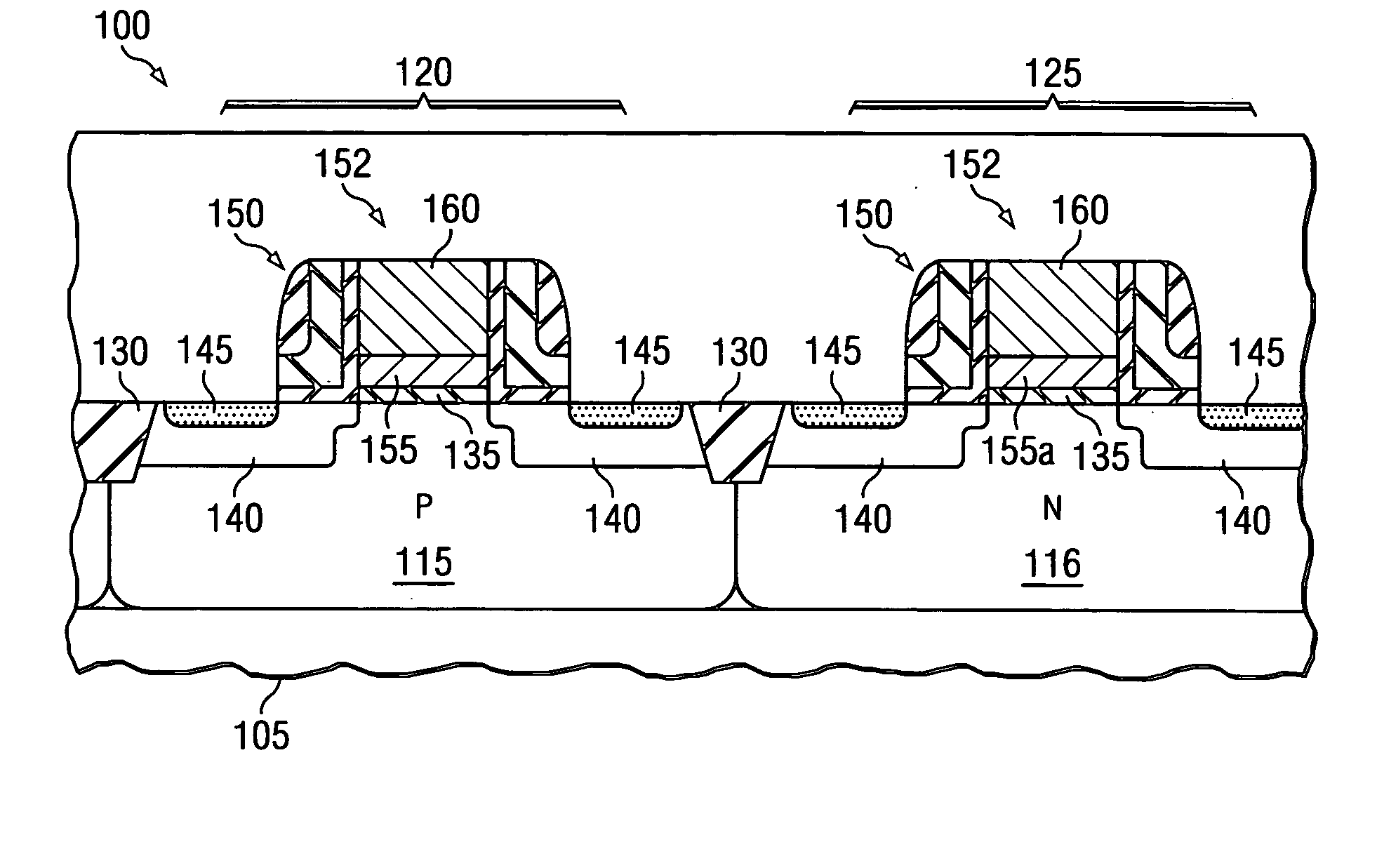
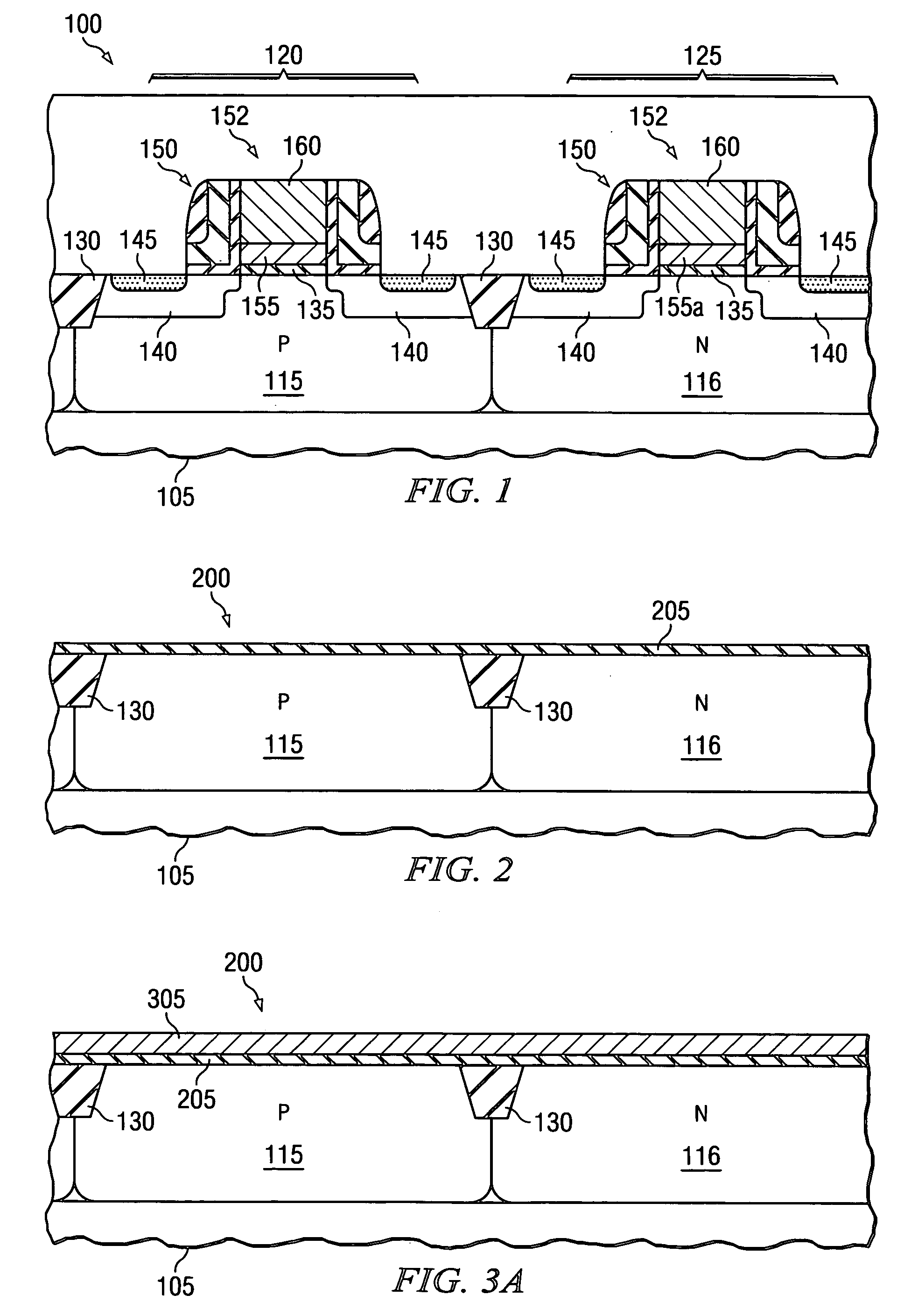
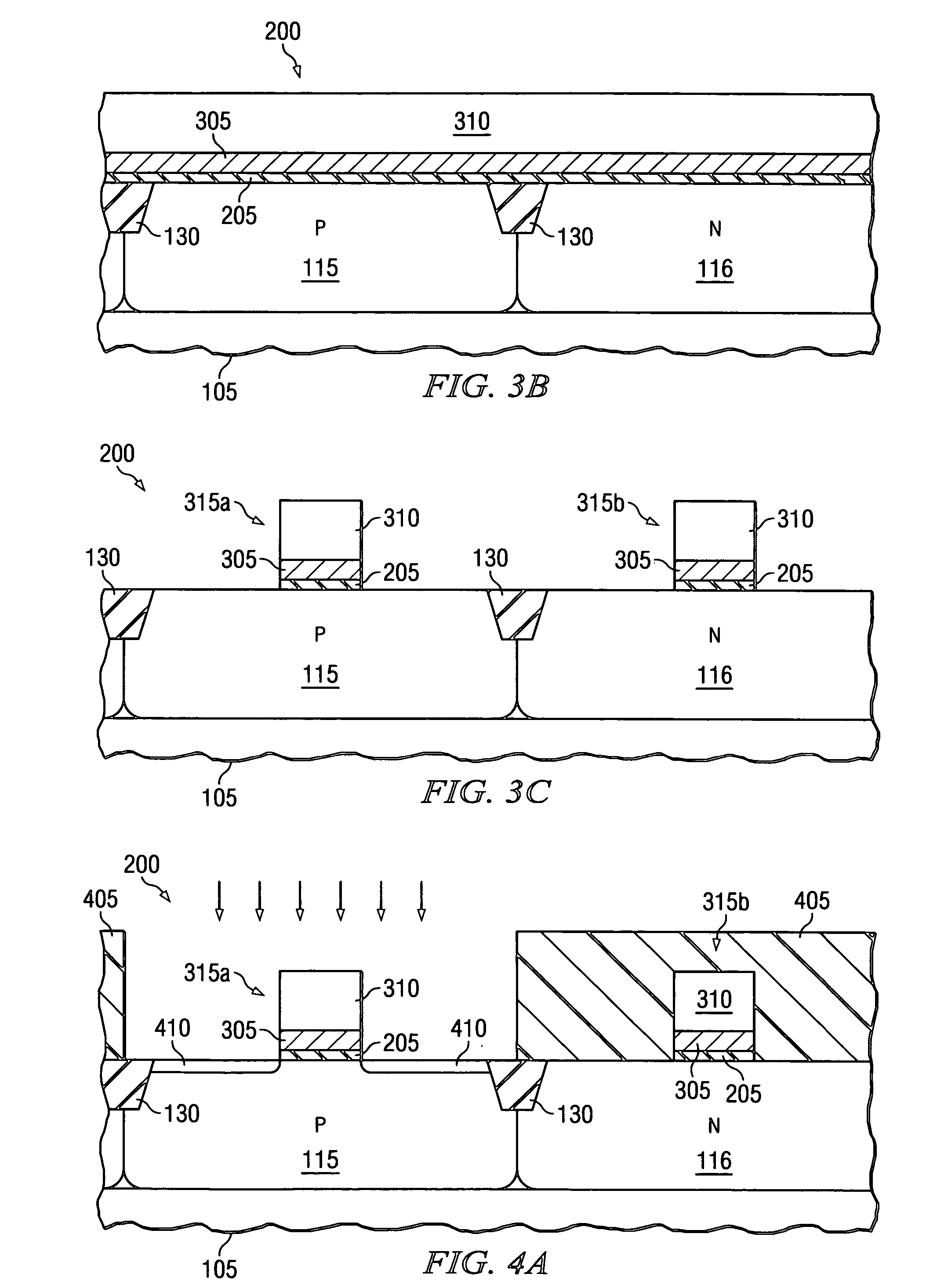
[0027] The present invention overcomes previous difficulties in the production of devices having dual work function metal gates by providing a process that allows for a high quality gate dielectric while deferring metal gate formation until after high thermal budgets are conducted, such as those conducted to form the gate dielectric, source / drains and silicided contacts. Moreover, because the metal gates are formed after the conduction of these high thermal processes, work function drift is minimized and metal combinations that formerly have been unavailable are now available for use in the metal gate formation. This process, therefore, provides for a high quality gate dielectric while avoiding work function drift within the metal gates. Such dual gate configurations facilitate work function control of the gates to enable dual gate microelectronic devices to be constructed with lower threshold voltages and higher reliability than previously obtainable.

[0028] The term, work functi...


PUM


Abstract

The present invention provides a method of forming a dual work function metal gate microelectronics device 200. In one aspect, the method includes forming nMOS and pMOS stacked gate structures 315a and 315b. The nMOS and pMOS stacked gate structures 315a and 315b each comprise a gate dielectric 205, a first metal layer, 305 located over the gate dielectric 205 and a sacrificial gate layer 310 located over the first metal layer 305. The method further includes removing the sacrificial gate layer 310 in at least one of the nMOS or pMOS stacked gate structures, thereby forming a gate opening 825 and modifying the first metal layer 305 within the gate opening 825 to form a gate electrode with a desired work function.

Description

TECHNICAL FIELD OF THE INVENTION [0001] The present invention is directed in general to a method for manufacturing microelectronic devices and, more specifically, to manufacturing dual work function metal gates for microelectronic devices. BACKGROUND [0002] The ability to dope polysilicon gates to different degrees allows one to adjust the work function of gate electrode materials to particular types of metal oxide silicon (MOS) transistors. It is desirable to adjust the work function of a gate electrode (hereinafter, the gate), to be close to either the conduction band or the valence band of silicon, because this reduces the threshold voltage (Vt) of the transistor, thereby facilitating a high drive current at low operating voltages. For instance, dual work function gates, for example doped polysilicon are advantageously used in microelectronic devices, such as complementary metal oxide silicon (CMOS) transistor devices, having both pMOS and nMOS transistors. The use of doped polys...

Claims


Application Information

Patent Timeline
IPC IPC(8): H01L21/8238
CPCH01L21/823842H01L29/66545
Inventor COLOMBO, LUIGICHAMBERS, JAMES J.VISOKAY, MARK R.
Owner TEXAS INSTR INC
Why Eureka
Try Eureka