Semiconductor device that is advantageous in operational environment at high temperatures

a technology of semiconductor devices and high temperature, applied in semiconductor devices, digital storage, instruments, etc., can solve the problems of reducing the mobility of electrons or holes (carriers), increasing the heat emitted from transistors, and becoming more and more sever

Inactive Publication Date: 2007-03-01
KK TOSHIBA
View PDF2 Cites 19 Cited by
  • Summary
  • Abstract
  • Description
  • Claims
  • Application Information

AI Technical Summary

Benefits of technology

[0009] According to an aspect of the present invention, there is provided a semiconductor device comprising: an N-type insulated-gate field-effect transistor including a first insulating layer that is provided along side walls of a gate electrode, has a negative expansion coefficient, and applies a tensile stress to a channel region of t...

Problems solved by technology

Being in direct proportion to the integration level, the heat emitted from the transistors becomes more and more intensive as the number of the transistors increases.
As a result, the degree of lattice vibration of the crystal lattice of, e.g. silicon that forms...

Method used


Image

  • Semiconductor device that is advantageous in operational environment at high temperatures
  • Semiconductor device that is advantageous in operational environment at high temperatures
  • Semiconductor device that is advantageous in operational environment at high temperatures

Examples


first embodiment

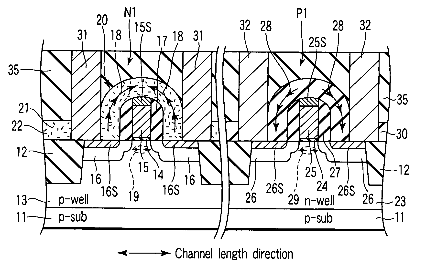
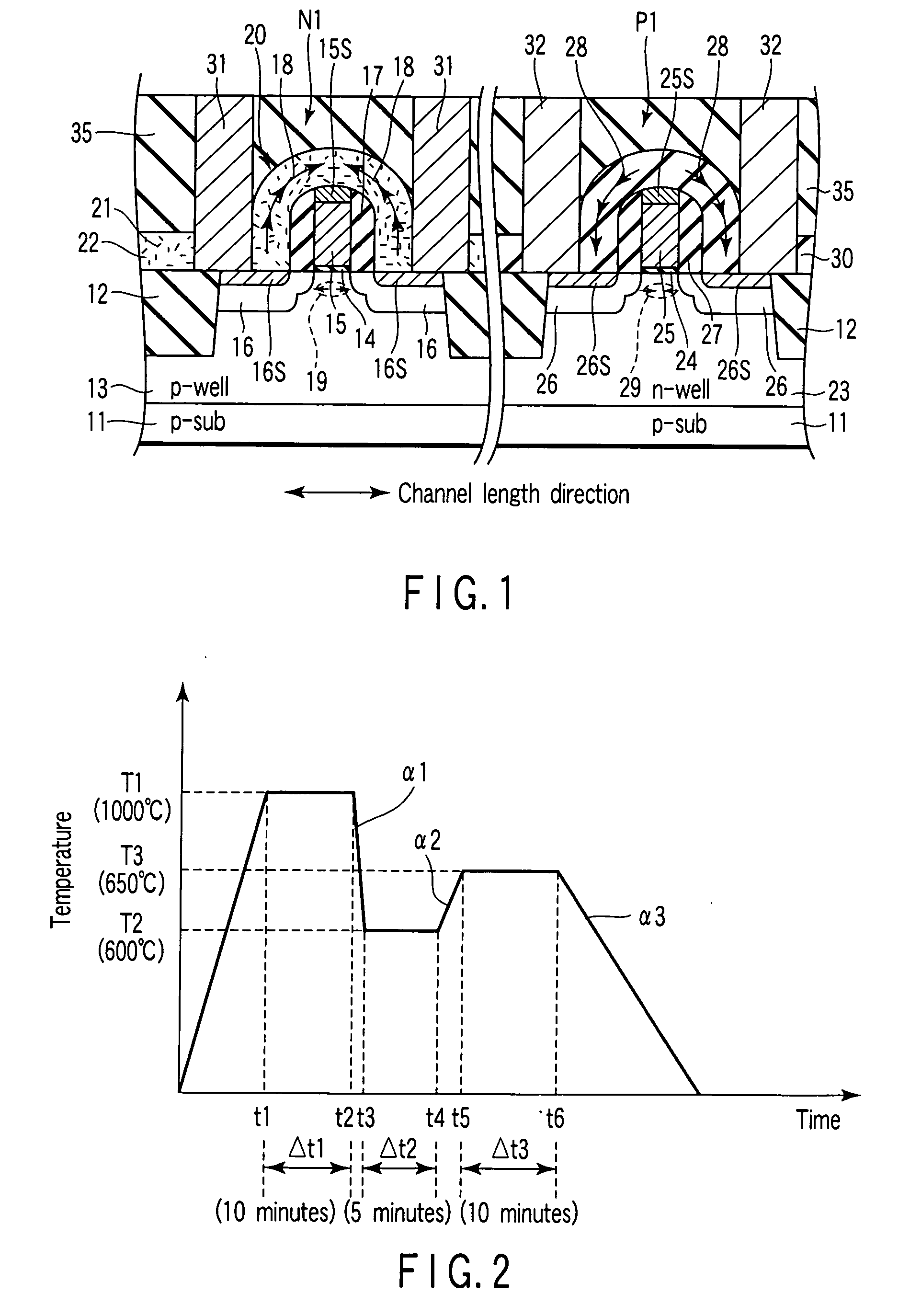
[0030] A semiconductor device according to a first embodiment of the present invention is described with reference to FIG. 1. FIG. 1 is a cross-sectional view that schematically shows the semiconductor device according to the first embodiment.

[0031] As is shown in FIG. 1, an NMOS transistor N1 that is an N-type MOS transistor is provided on a P-well (p-well) 13 in a P-type semiconductor (e.g. silicon) substrate (p-sub) 11, which is isolated by a device isolation film 12. A PMOS transistor P1 that is a P-type MOS transistor is provided on an N-well (n-well) 23 in the same substrate 11. An interlayer insulation film 35 is provided so as to cover the transistors N1 and P1.

[0032] The NMOS transistor N1 comprises a gate insulation film 14, a gate electrode 15, source / drain regions 16, silicide layers 15S and 16S, spacers 17, an insulating layer 20, and source / drain contact plugs 31.

[0033] The gate insulation film 14 is provided on the P-well 13 in the semiconductor substrate 11. The g...

second embodiment

[0094] A semiconductor device according to a second embodiment of the invention is described with reference to FIG. 11. A description of the parts that are common to those in the first embodiment is omitted.

[0095] As is shown in FIG. 11, an NMOS transistor N2 is provided on the P-well 13 in the semiconductor substrate 11, and a PMOS transistor P1 is provided on the N-well 23.

[0096] The semiconductor device of the second embodiment differs from that of the first embodiment in that a HfW2O8 layer 61 is provided, as an insulating layer with a negative thermal expansion coefficient, over the silicide layers 16S, spacers 17 and silicide layer 15S. The HfW2O8 layer 61 has an thermal expansion coefficient of about −10×10−6 / K in a range between room temperature and about 800K.

[0097] Accordingly, when the temperature of the transistor N2 rises in operation, the HfW2O8 layer 61 contracts and a stress 18 occurs in a direction from the source / drain regions 16 towards the silicide layer 15S. ...

third embodiment

[0114] A semiconductor device according to a third embodiment of the invention is described with reference to FIG. 14. A description of the parts that are common to those in the first embodiment is omitted.

[0115] As is shown in FIG. 14, a PMOS transistor P2 is provided on the N-well 23. The third embodiment differs from the first embodiment in that an Al2O3 layer 71 is provided as an insulating layer over the silicide layers 26S, spacers 27 and silicide layer 25S. The Al2O3 layer 71 has a positive thermal expansion coefficient.

[0116] The fabrication method is substantially the same as that in the first embodiment, so a detailed description is omitted here.

[0117] According to the semiconductor device of this embodiment and the fabrication method thereof, the same advantageous effects as in the first embodiment can be obtained. Further, in the semiconductor device of this embodiment, the Al2O3 layer 71 is provided as the insulating layer of the PMOS transistor P2. The magnitude of ...


PUM


Abstract

A semiconductor device comprises an N-type insulated-gate field-effect transistor including a first insulating layer that is provided along side walls of a gate electrode, has a negative thermal expansion coefficient, and applies a tensile stress to a channel region of the N-type insulated-gate field-effect transistor. The device also comprises a P-type insulated-gate field-effect transistor including a second insulating layer that is provided along side walls of a gate electrode, has a positive thermal expansion coefficient, and applies a compression stress to a channel region of the P-type insulated-gate field-effect transistor.

Description

CROSS-REFERENCE TO RELATED APPLICATIONS [0001] This application is based upon and claims the benefit of priority from prior Japanese Patent Application No. 2005-249752, filed Aug. 30, 2005, the entire contents of which are incorporated herein by reference. BACKGROUND OF THE INVENTION [0002] 1. Field of the Invention [0003] The present invention relates generally to a semiconductor device, and the invention is applicable to, e.g. a transistor in which the mobility of electrons or holes is varied by applying a stress to a semiconductor substrate. [0004] 2. Description of the Related Art [0005] In the prior art, as one of active devices that constitute an LSI (large-scale integration), there is known an insulated-gate field-effect transistor (hereinafter referred to as “transistor”) that is represented by a MOS (metal oxide semiconductor) transistor or a MIS (metal insulator semiconductor) transistor. With development in fine patterning of the transistors, the number of transistors in ...

Claims


Application Information

Patent Timeline
IPC IPC(8): H01L29/10
CPCH01L21/823807H01L29/7843H01L21/823864H01L21/76834
Inventor JIN, ZHENGWU
Owner KK TOSHIBA
Why Eureka
Try Eureka