
Eureka
For R&D, Eureka makes reading and utilizing patents & technical documents easy.
Eureka AIR
Designed for self-driven R&D workflows. Generate viable solutions, solve complex R&D challenges, empower your innovation with AI.

Eureka Materials
Designed for material experts only. Revolutionize your material R&D, from search, analyze, to developing new materials.

TechResearch
Generate reliable direction feasibility study reports for your R&D in just a few steps.

TechSeek
Discover and master advanced knowledge NOW. Basics, ideas, possibilities, all at once.

TechMind
As an expert in R&D Theories, TechMind can generates customized viable solutions instantly.

TechRisk
Analyze your overall solution with one click, know your potential R&D risks in advance.

TechMonitor
Get weekly tech updates, stay abreast of the latest tech innovations and key insights.
Surface mount optoelectronic component with lens
- Summary
- Abstract
- Description
- Claims
- Application Information
AI Technical Summary
Benefits of technology
Problems solved by technology
Method used
Image

Examples
Embodiment Construction
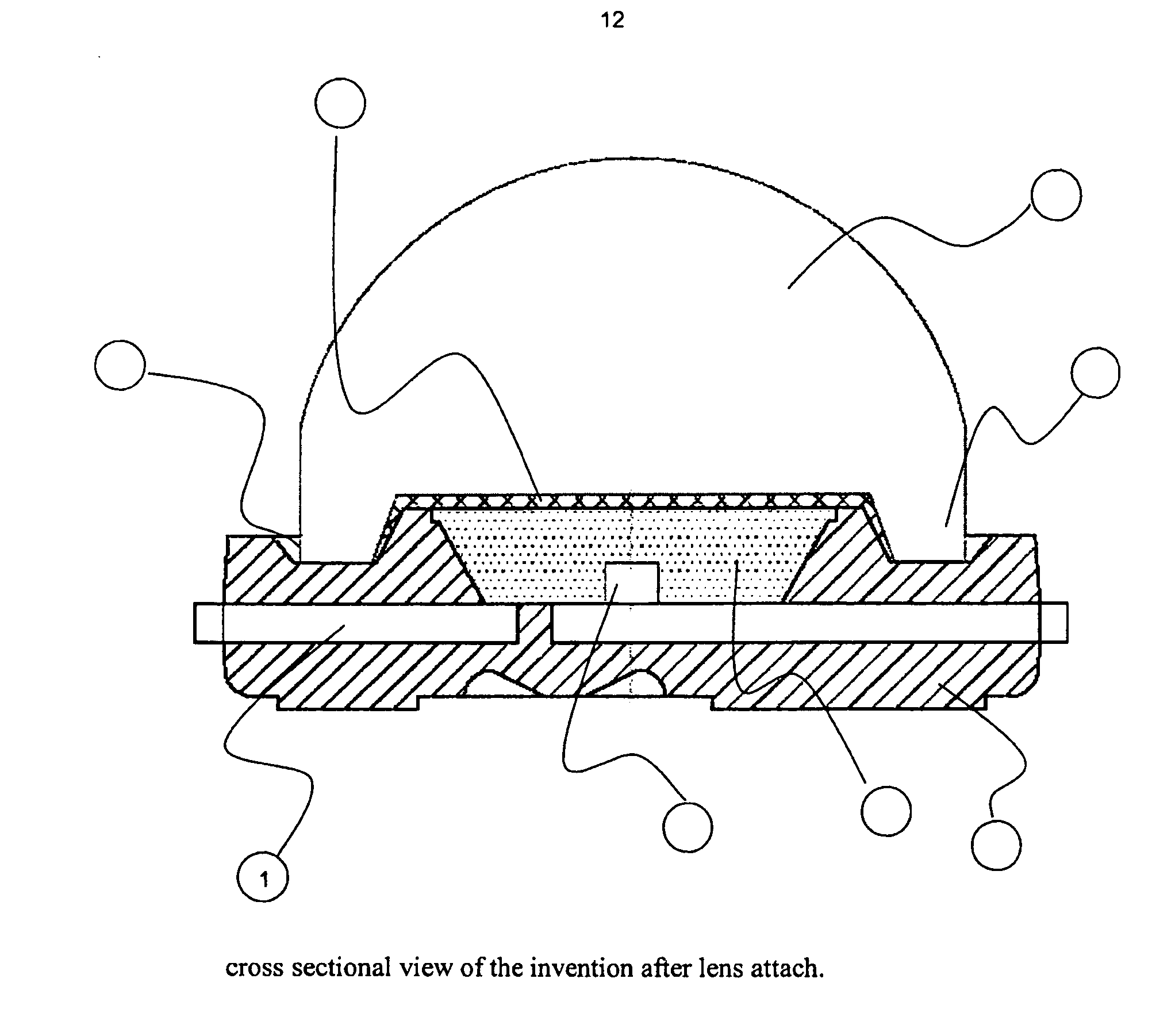
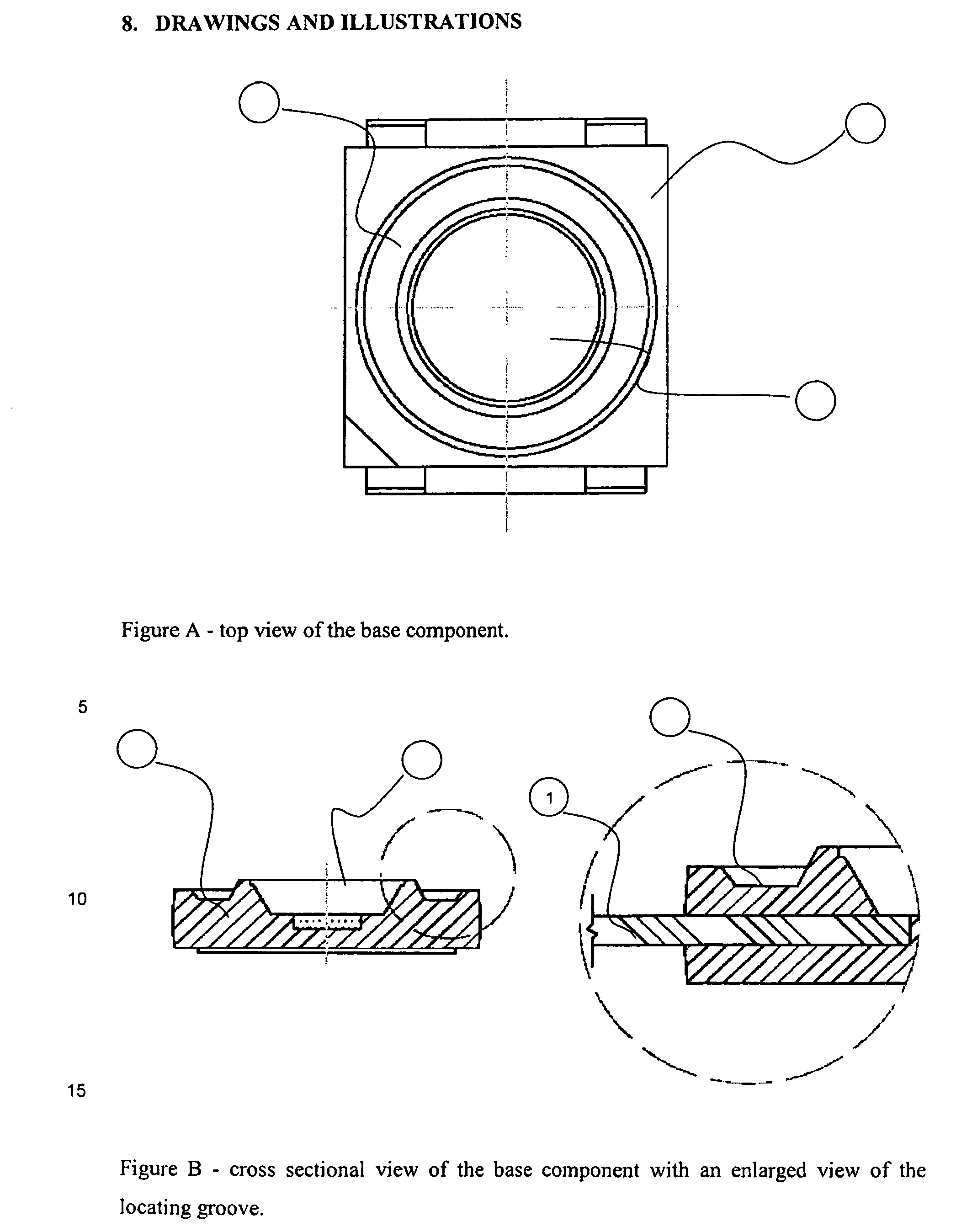
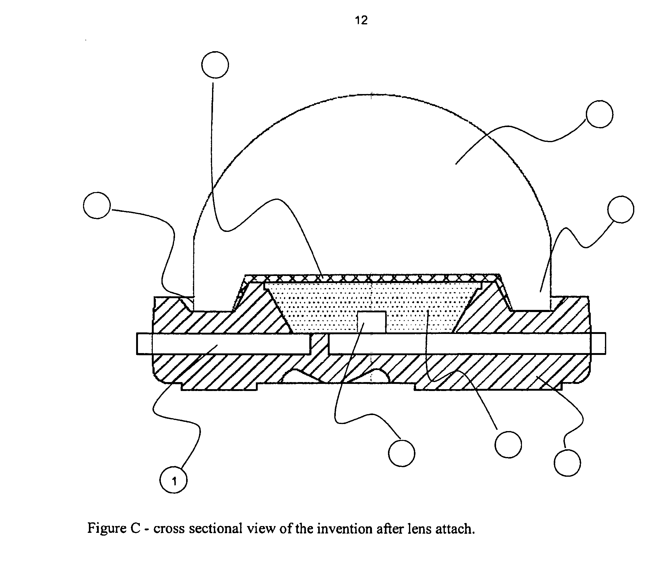
[0042] In an embodiment of the present invention, the optoelectronic component based on the surface mount technology is made up of a thick electrically conductive material which is used to serve as the base for the assembly an opaque plastic material which is used to provide the housing for the whole component and a cavity designed within the plastic material where an optoelectronic chip is mounted within. Multiple chips may also be mounted if required. This cavity is filled with a encapsulation material so that optical radiation may be transmitted or received via this material. Electrical connection(s) between the chip / chips and the base material is provided by a metallic wire.
[0043] The housing of the base component is designed in such a way whereby a groove is formed around the cavity. This groove is used to position the lens which is attached onto the base component. On the lens itself, a protruding structure is made to locate into the groove found on the base component. The ar...
PUM
 Abstract
Description
Claims
Application Information
 - R&D Engineer
- R&D Manager
- IP Professional
- Industry Leading Data Capabilities
- Powerful AI technology
- Patent DNA Extraction
Browse by: Latest US Patents, China's latest patents, Technical Efficacy Thesaurus, Application Domain, Technology Topic, Popular Technical Reports.
© 2024 PatSnap. All rights reserved.Legal|Privacy policy|Modern Slavery Act Transparency Statement|Sitemap|About US| Contact US: help@patsnap.com