Multiplication circuitry

a multiplication circuit and circuit technology, applied in the field of multiplication circuits, can solve the problems of strict demands, lack of flexibility in input timing and output timing of full adders, etc., and achieve the effect of reducing the severity of the timing requirements of inputs and lessening timing constraints

Inactive Publication Date: 2007-03-01
STMICROELECTRONICS (RES & DEV) LTD
View PDF1 Cites 2 Cited by
  • Summary
  • Abstract
  • Description
  • Claims
  • Application Information

AI Technical Summary

Benefits of technology

[0011] To address the above-discussed deficiencies of the prior art, an object of the present invention is to reduce the severity of the timing requirements of the inputs and therefore lessening the timing constraints imposed on previous stages of the binary multiplier with respect to multiplication of binary numbers.
[0013] Embodiments of the invention described in the following have the advantage of lowering the timing constraints imposed on the use of the combined bit groups, as the first combined bit group is produced by circuitry before the production of the second combined bit group. This allows the further combination circuit stages to take advantage of the early supply of combined bits to produce timing advantages for the data flow path.
[0016] Embodiments of the invention described hereafter have the further advantage whereby the arrangement of the stages benefits from the staggering of the inputs and outputs between stages to significantly reduce the critical path length for compression data.

Problems solved by technology

These conventional stages comprising full adders lack flexibility in both input timing and output timing, requiring the timing of inputs to be strictly controlled and therefore producing strict demands on the circuitry generating the prior stages and also producing the partial product terms initially input to the compression circuit.

Method used


Image

  • Multiplication circuitry
  • Multiplication circuitry
  • Multiplication circuitry

Examples


Embodiment Construction

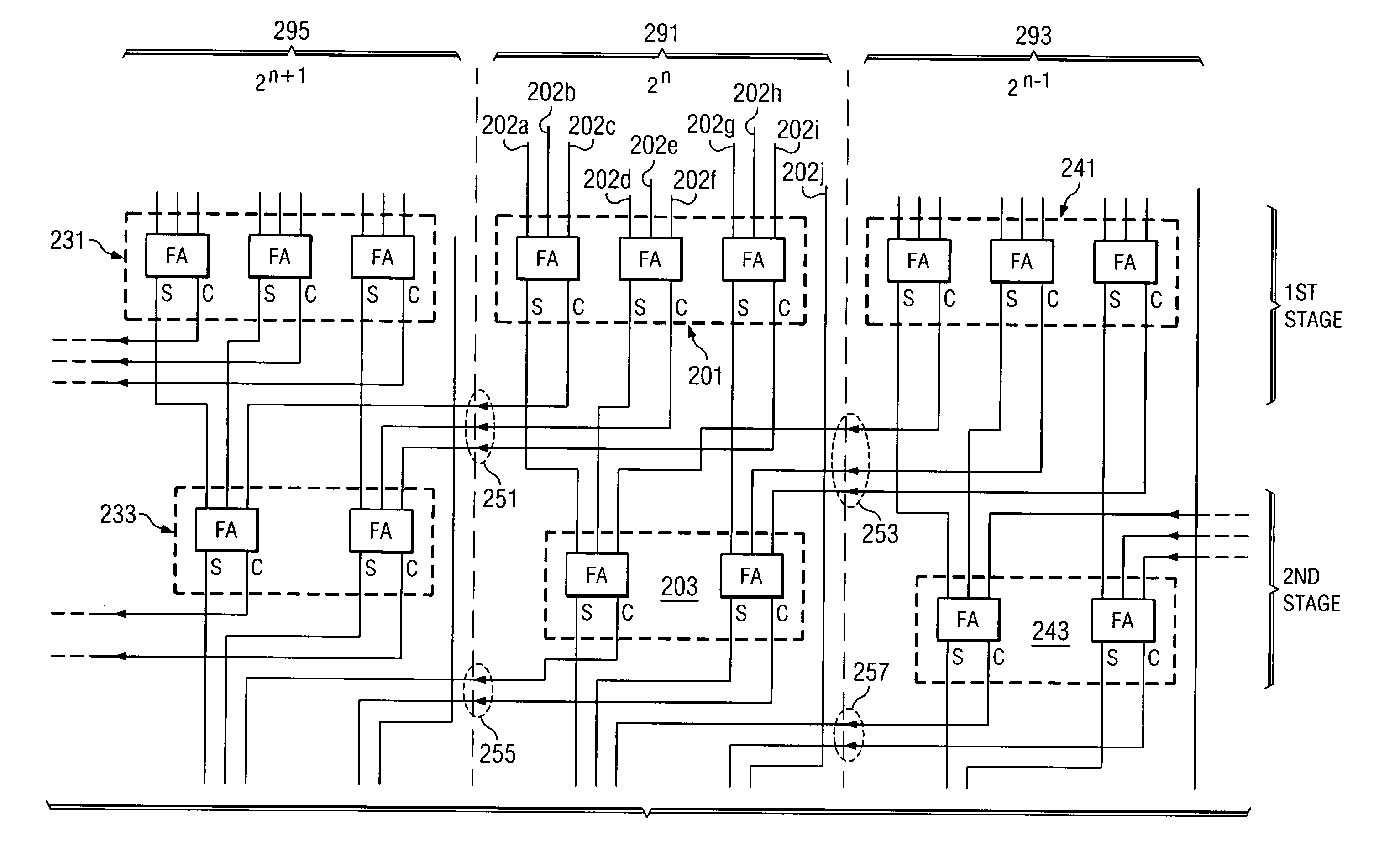
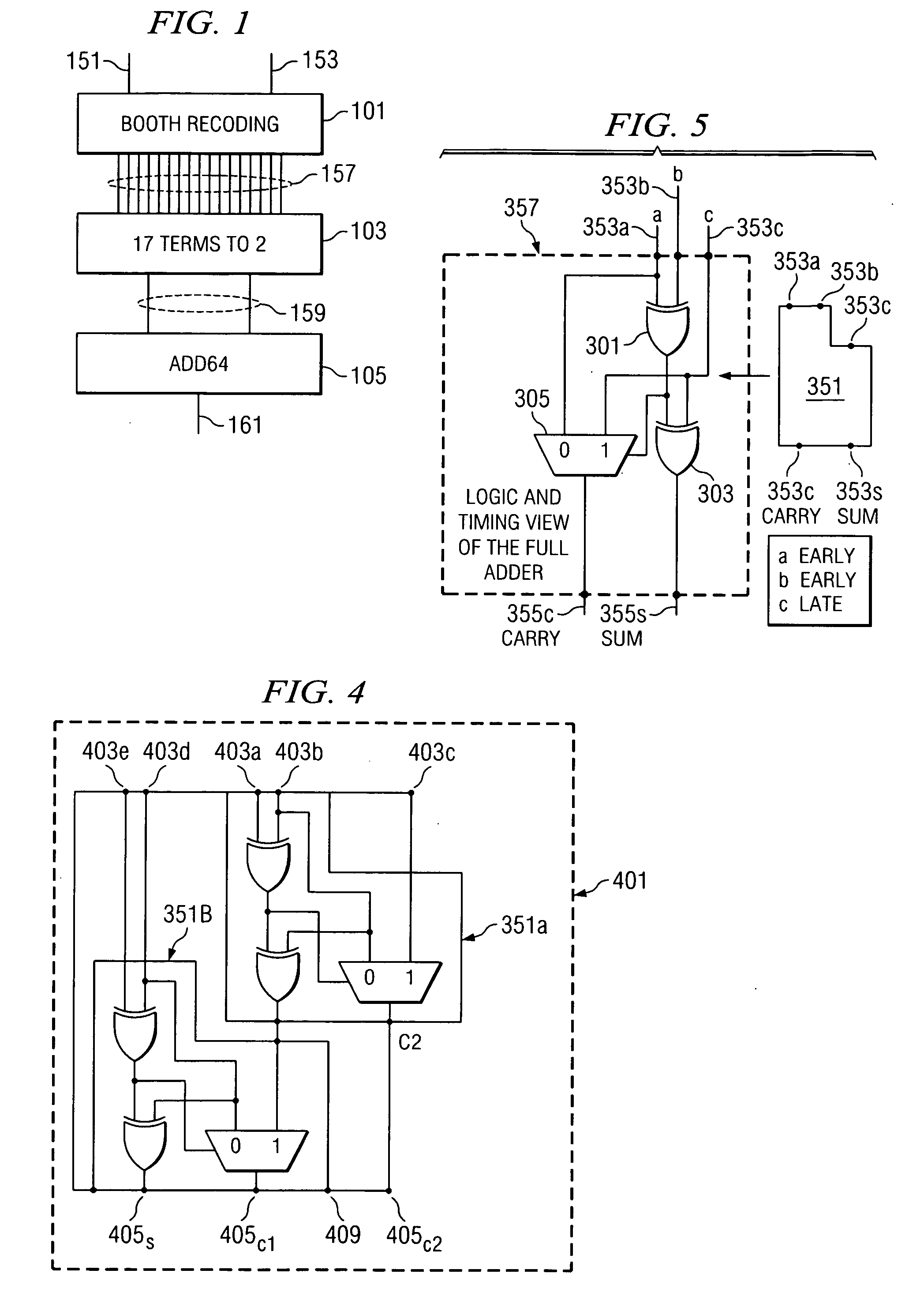
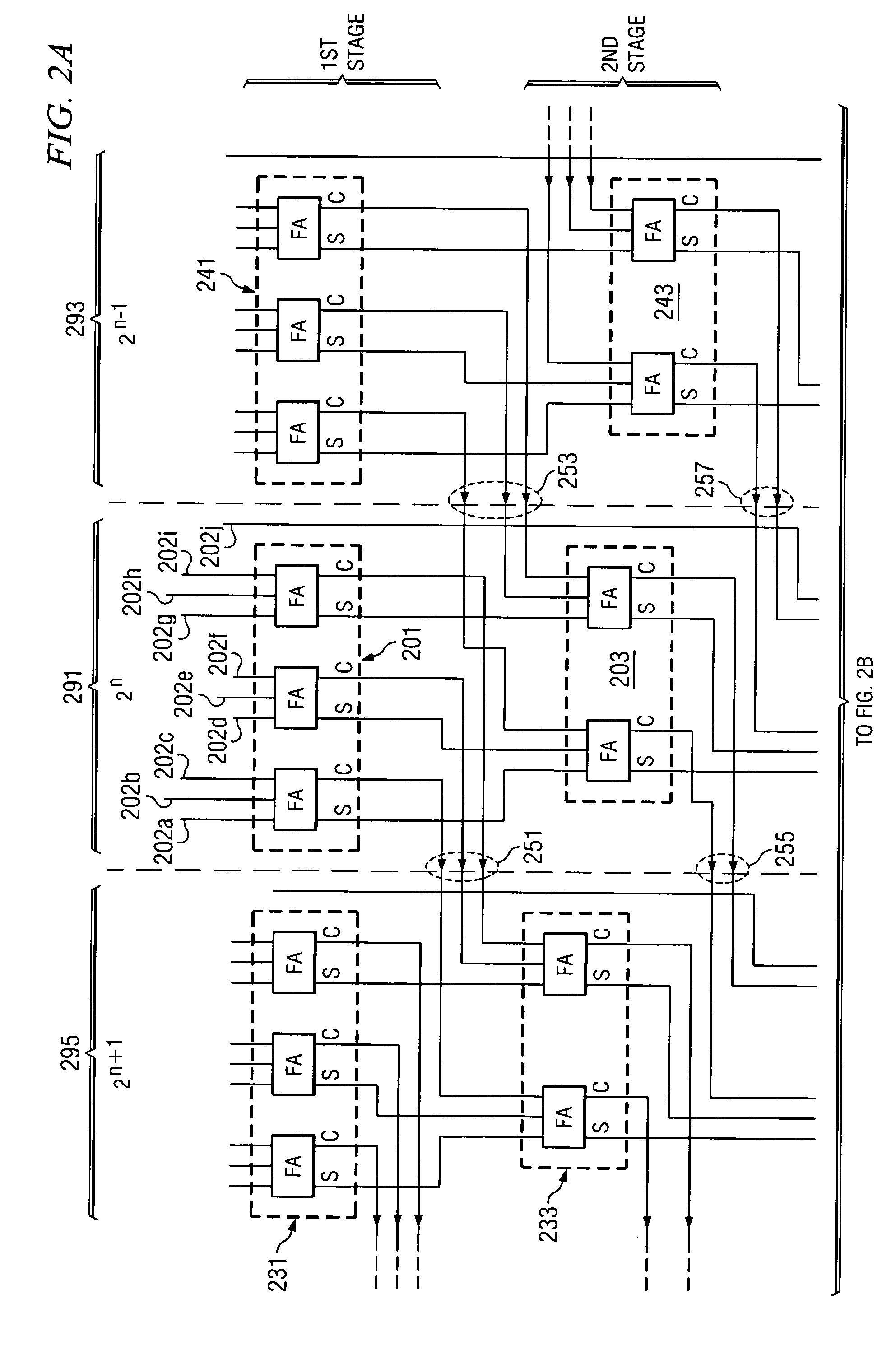
[0032]FIGS. 2 through 6, discussed below, and the various embodiments used to describe the principles of the present invention in this patent document are by way of illustration only and should not be construed in any way to limit the scope of the invention. Those skilled in the art will understand that the principles of the present invention may be implemented in any suitably arranged circuitry.

[0033] The encoding, partial product generation, and addition stages of the multiplication circuits as known in the art are not described in further detail. For the examples described with reference to FIGS. 2 and 3, a compression column circuit is shown which receives the output from a Booth encoding algorithm, which generates 10 partial products. With reference to FIG. 6, a compression column circuit receives an output from a Booth encoding algorithm which generates 25 partial products.

[0034] As appreciated by a person skilled in the art, the examples described below with reference to 10...


PUM


Abstract

Combination circuitry for combining a plurality of multi-bit partial product terms includes at least one stage arranged to receive a first number of input bits. At least one stage includes at least one combiner having: a first logic device comprising an input arranged to receive a first set of the first number of input bits and an output arranged to output a first combined result; a second logic device comprising a first input arranged to receive a second set of the first number of input bits, a second input connected to receive the first combined result, a first output arranged to output a second combined result, and a second output arranged to output a first combined bit group; and a third logic device comprising an input connected to receive the second combined result and an output arranged to output a second combined bit group, whereby the first combined bit group is available for a further stage of the combination circuitry before the second combined bit group.

Description

TECHNICAL FIELD OF THE INVENTION [0001] The present invention relates to combination circuitry, particularly but not exclusively for multiplication circuitry. BACKGROUND OF THE INVENTION [0002] A typical binary multiplier for multiplying two binary numbers together comprises a series of processing stages, such as an operand encoder, a partial product generator, a product term compressor, and a final addition stage. [0003] The operand encoder encodes the first operand and reduces the number of terms representing the operand. Thus, for example, a 32-bit number may be reduced using a Booth code to 17 terms or fewer. [0004] The partial product generator multiplies the second operand by each of the encoded terms to produce a partial product term. Thus, for a 32-bit multiplier where the first operand is encoded as 17 terms, a total of 17 partial product terms are produced. [0005] The product term compressor adds together (or as otherwise known compresses) the many partial products to form...

Claims


Application Information

Patent Timeline
Patent Type & Authority Applications(United States)
IPC IPC(8): H03M7/34
CPCG06F7/5318
Inventor KURD, TARIQ
Owner STMICROELECTRONICS (RES & DEV) LTD
Why Eureka
Try Eureka