Flash memory device with improved read speed

a flash memory and read speed technology, applied in static storage, digital storage, instruments, etc., can solve the problems of inability to erase one memory cell at a time, lack of endurance, wear and tear, etc., to improve read performance, improve read performance, and reduce development time

Inactive Publication Date: 2007-03-01
SAMSUNG ELECTRONICS CO LTD
View PDF6 Cites 43 Cited by
  • Summary
  • Abstract
  • Description
  • Claims
  • Application Information

AI Technical Summary

Benefits of technology

[0013] Recognizing the need to improve the read performance in multi-bit (or “multi-level”) flash cells, embodiments of the present invention provide multi-bit flash memory devices capable of improving the read performance by reducing the develop time.

Problems solved by technology

Some of flash memory's drawbacks include its tendency to wear out over time (lack of endurance), the inability to erase one memory cell at a time, and its relatively low degree of integration and speed compared with various forms of volatile memory such as dynamic random access memory (DRAM) and static random access memory (SRAM).
Moreover, the develop time also tends to increase the time required for the read operation of the multi-bit cell.

Method used


Image

  • Flash memory device with improved read speed
  • Flash memory device with improved read speed
  • Flash memory device with improved read speed

Examples


Embodiment Construction

[0025] Exemplary embodiments of the invention are described below with reference to the corresponding drawings. These embodiments are presented as teaching examples. The actual scope of the invention is defined by the claims that follow.

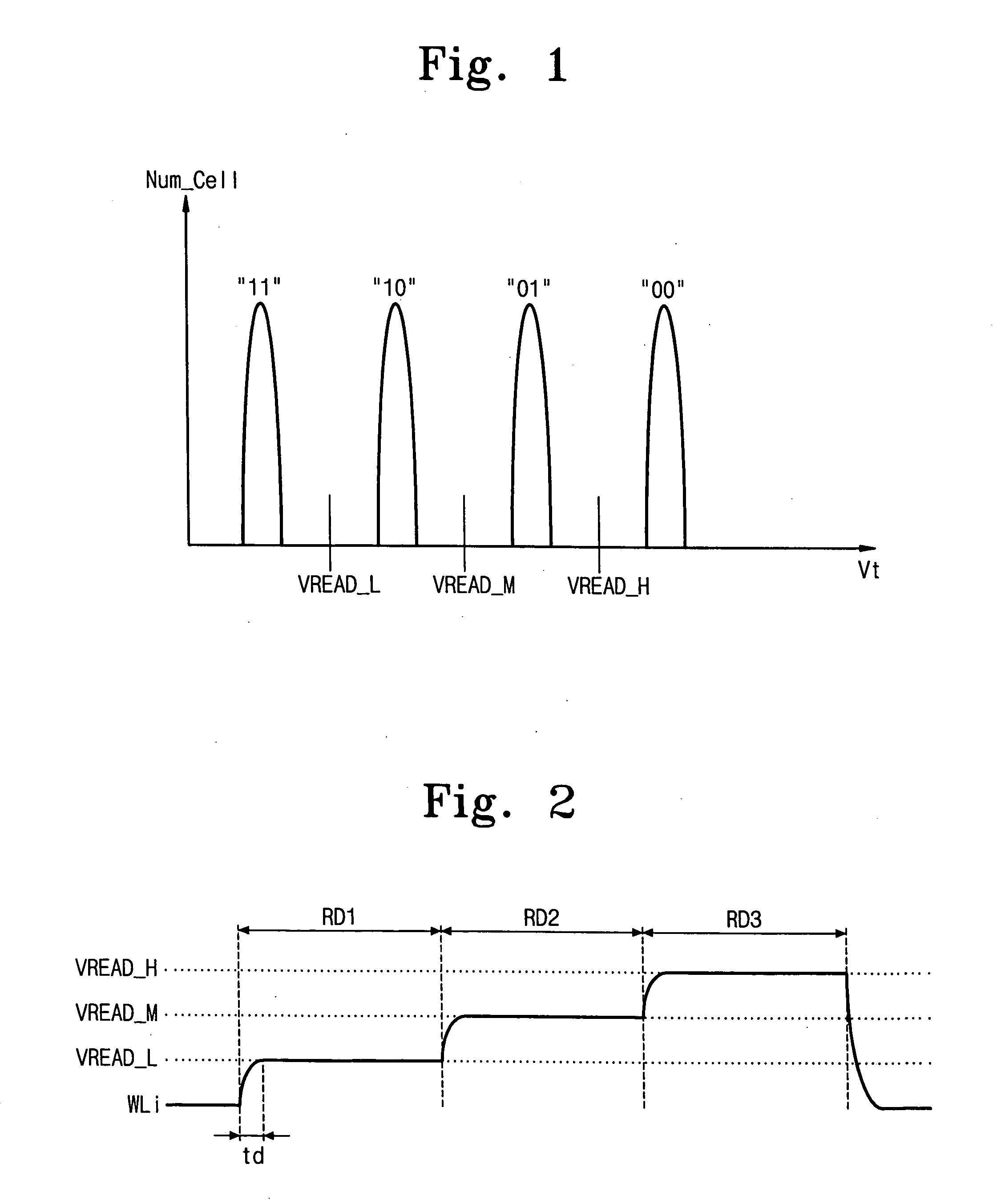
[0026] In this written description, the term “read operation” is used to describe a process for reading multiple bits of information from a nonvolatile memory cell. For example, a read operation may be used to read 2-bit data from a memory cell during first, second and third read periods.

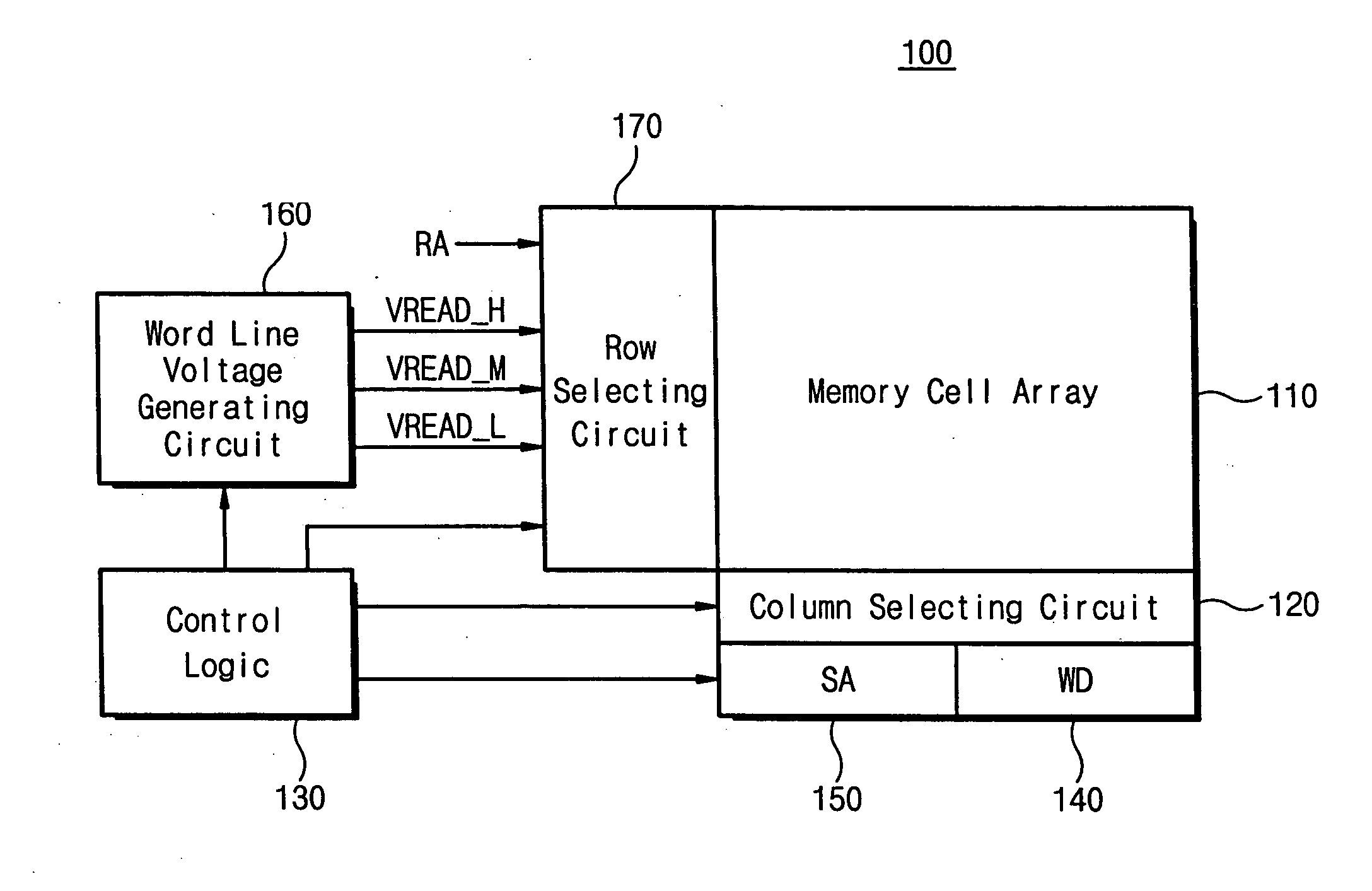
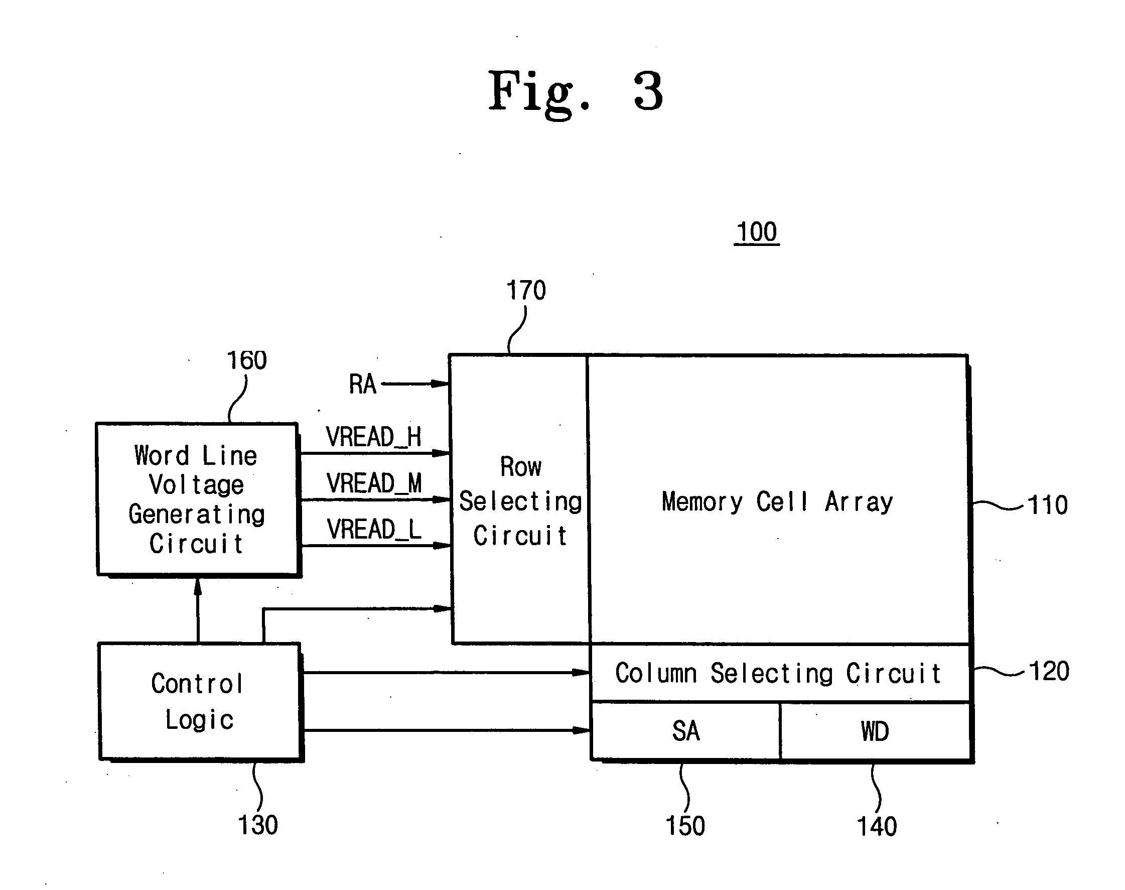
[0027]FIG. 3 is a block diagram of a flash memory device 100 according to one embodiment of the present invention. The flash memory device shown in FIG. 3 is preferably a NOR flash memory device. However, those skilled in the art will recognize that the memory device of FIG. 3 could be alternatively configured to use other types of nonvolatile memory such as masked read only memory (MROM), programmable read only memory (PROM), ferroelectric random access memory (FR...


PUM


Abstract

A flash memory device comprises an array of memory cells arranged in rows and columns and a word line voltage generating circuit adapted to generate a plurality of read voltages at the same time during a multi-bit read operation. The device further comprises a row selecting circuit adapted to select one of the rows and drive the selected row with a word line voltage, and voltage lines transmitting the respective read voltages to the row selecting circuit as the word line voltage. The read voltages are supplied to the respective voltage lines before starting read periods of the multi-bit read operation.

Description

BACKGROUND OF THE INVENTION [0001] 1. Field of the Invention [0002] Embodiments of the present invention relate generally to a semiconductor memory device. More particularly, embodiments of the invention relate to a flash memory device having multi-bit memory cells. [0003] This application claims the priority of Korean Patent Application No. 2005-78372, filed Aug. 25, 2005, the disclosure of which is hereby incorporated by reference in its entirety. [0004] 2. Description of Related Art [0005] Flash memory is a popular form of non-volatile memory used in many modern electronic devices. Functionally, flash memory is a type of electrically erasable programmable read only memory (EEPROM) where memory cells can be programmed or read individually, but must be erased in units called “blocks.” Flash memory can be found in a wide range of consumer and industrial electronic devices, from personal computers (PCs) and removable disk drives to cameras, cellular phones, and personal digital assis...

Claims


Application Information

Patent Timeline
Patent Type & Authority Applications(United States)
IPC IPC(8): G11C16/04
CPCG11C16/26G11C11/5642G11C5/14G11C8/08G11C16/08G11C16/30
Inventor LEE, DOO-SUBLIM, HEUNG-SOO
Owner SAMSUNG ELECTRONICS CO LTD
Why Eureka
Try Eureka